
User Manual


GSM/GPRS Module Series
GC10 Hardware Design
GC10_Hardware_Design Confidential / Released 19 / 76
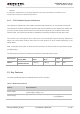
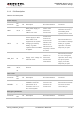
UART Port
Pin Name
Pin
NO.
I/O
Description DC Characteristics Comment
RI 6 O Ring indication
VILmin=0V
VILmax=
0.3×VDD_EXT
VIHmin=
0.7×VDD_EXT
VIHmax=
VDD_EXT
VOLmin=0V
VOLmax=
0.3×VDD_EXT
VOHmin=
0.7×VDD_EXT
VOHmax=
VDD_EXT
If only use TXD, RXD
and GND to
communicate,
recommended
connecting RTS to
GND via a 0R resistor
and keeping other pins
open.
DTR 7
I
Data terminal ready
DCD 8 O Data carrier detection
TXD 9 O Transmit data
RXD 10 I Receive data
RTS 11 I Request to send
CTS 12 O Clear to send
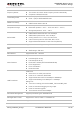
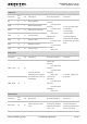
Debug Port
Pin Name
Pin
NO.
I/O
Description DC Characteristics Comment
DBG_TXD 31 O
Used for firmware
debugging and upgrade.
The baud rate is fixed at
921600bps.
VILmin=0V
VILmax=
0.3×VDD_EXT
VIHmin=
0.7×VDD_EXT
VIHmax=
VDD_EXT
VOLmin=0V
VOLmax=
0.3×VDD_EXT
VOHmin=
0.7×VDD_EXT
VOHmax=
VDD_EXT
If unused, keep these
pins open.
DBG_RXD 30 I
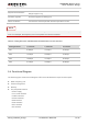
SIM Interface
Pin Name
Pin
NO.
I/O
Description DC Characteristics Comment
SIM_VDD 23 O
Power supply for SIM
card
The voltage can be
selected by software
automatically. Either
1.8V or 3V.
All signals of SIM
interface should be
protected against ESD
with a TVS diode