
User Manual


GSM/GPRS Module Series
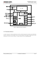
GC10 Hardware Design
GC10_Hardware_Design Confidential / Released 17 / 76
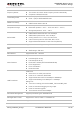
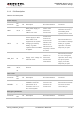
3.1.2. Pin Description
Table 3: Pin Description
Power Supply
Pin Name
Pin
NO.
I/O
Description DC Characteristics Comment
VBAT 33,34 I
Main power supply of
module:
VBAT=3.3V~4.6V
Vmax= 4.6V
Vmin=3.3V
Vnorm=4.0V
Make sure that supply
sufficient current in a
transmitting burst
typically rises to 1.6A.
VRTC 13 I/O
Power supply for RTC
when VBAT is not
supplied for the system.
Charging for backup
battery or golden
capacitor when the VBAT
is applied.
VImax=3.3V
VImin=2.0V
VInorm=2.8V
VOmax=2.9V
VOmin=2.7V
VOnorm=2.8V
Iout(max)=1.35mA
Iin=70uA
Recommended to be
connected to a backup
battery or a golden
capacitor. If unused,
keep this pin open.
VDD_EXT 29 O
Supply 3.0V voltage for
external circuit.
Vmax=3.1V
Vmin=2.9V
Vnorm=3.0V
Imax=20mA
Recommend to add a
2.2 or 4.7uF bypass
capacitor, when using
this pin for power
supply. If unused,
keep this pin open.
GND
32,35,
36,37,
39
Ground
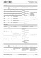
Turn on/off
Pin Name
Pin
NO.
I/O
Description DC Characteristics Comment
PWRKEY 5 I
Power on/off key.
PWRKEY should be
pulled down for a
moment to turn on or
turn off the system.
VILmax=2.0V
VIHmin=2.3V
VImax=3.3V
Recommend to add an
OC driver circuit to
control this pin.
Emergency Shutdown
Pin Name
Pin
NO.
I/O
Description DC Characteristics Comment