
User Manual


GSM/GPRS Module Series
GC10 Hardware Design
GC10_Hardware_Design Confidential / Released 13 / 76
When the module works within this temperature range, the deviations from the GSM specification may
occur. For example, the frequency error or the phase error will be increased.
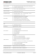
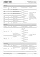
Table 2: Coding Schemes and Maximum Net Data Rates over Air Interface
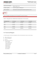
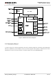
2.4. Functional Diagram
The following figure shows a block diagram of GC10 and illustrates the major functional parts.
Radio frequency part
Power management
Memory
The peripheral interface
—Power supply
—Turn-on/off interface
—UART interfaces
—Audio interfaces
—SIM interface
—PCM interface
—RTC interface
—RF interface
Physical Characteristics
Size: 19±0.15×16.9±0.15×2.35±0.2mm
Weight: Approx.1.3g
Firmware Upgrade Firmware upgrade via debug port
Antenna Interface Connected to antenna pad with 50 Ohm impedance control
Coding Scheme 1 Timeslot 2 Timeslot 4 Timeslot
CS-1 9.05kbps 18.1kbps 36.2kbps
CS-2 13.4kbps 26.8kbps 53.6kbps
CS-3 15.6kbps 31.2kbps 62.4kbps
CS-4 21.4kbps 42.8kbps 85.6kbps
NOTE