
User's Manual
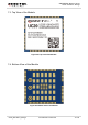

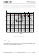
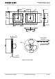
Table Of Contents
- About the Document
- Contents
- Table Index
- Figure Index
- 1 Introduction
- 2 Product Concept
- 3 Application Interface
- 3.1. General Description
- 3.2. Pin Assignment
- 3.3. Pin Description
- 3.4. Operating Modes
- 3.5. Power Saving
- 3.6. Power Supply
- 3.7. Turn on and off Scenarios
- 3.8. Reset the Module
- 3.9. RTC Backup
- 3.10. UART Interface
- 3.11. USIM Card Interface
- 3.12. USB Interface
- 3.13. PCM and I2C Interface
- 3.14. ADC Function
- 3.15. Network Status Indication
- 3.16. Operating Status Indication
- 3.17. Behavior of the RI
- 4 GNSS Receiver
- 5 Antenna Interface
- 6 Electrical, Reliability and Radio Characteristics
- 7 Mechanical Dimensions
- 8 Storage and Manufacturing
- 9 Appendix A Reference

UMTS/HSPA Module Series
UC20 Hardware Design
UC20_Hardware_Design Confidential / Released 80 / 84
V
IH
min
Minimum Input High Level Voltage Value
V
IL
max
Maximum Input Low Level Voltage Value
V
IL
min
Minimum Input Low Level Voltage Value
V
I
max
Absolute Maximum Input Voltage Value
V
I
min
Absolute Minimum Input Voltage Value
V
OH
max
Maximum Output High Level Voltage Value
V
OH
min
Minimum Output High Level Voltage Value
V
OL
max
Maximum Output Low Level Voltage Value
V
OL
min
Minimum Output Low Level Voltage Value
VSWR
Voltage Standing Wave Ratio
WCDMA
Wideband Code Division Multiple Access