
User's Manual
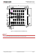
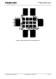
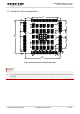
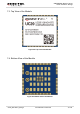

Table Of Contents
- About the Document
- Contents
- Table Index
- Figure Index
- 1 Introduction
- 2 Product Concept
- 3 Application Interface
- 3.1. General Description
- 3.2. Pin Assignment
- 3.3. Pin Description
- 3.4. Operating Modes
- 3.5. Power Saving
- 3.6. Power Supply
- 3.7. Turn on and off Scenarios
- 3.8. Reset the Module
- 3.9. RTC Backup
- 3.10. UART Interface
- 3.11. USIM Card Interface
- 3.12. USB Interface
- 3.13. PCM and I2C Interface
- 3.14. ADC Function
- 3.15. Network Status Indication
- 3.16. Operating Status Indication
- 3.17. Behavior of the RI
- 4 GNSS Receiver
- 5 Antenna Interface
- 6 Electrical, Reliability and Radio Characteristics
- 7 Mechanical Dimensions
- 8 Storage and Manufacturing
- 9 Appendix A Reference

UMTS/HSPA Module Series
UC20 Hardware Design
UC20_Hardware_Design Confidential / Released 79 / 84
PCB
Printed Circuit Board
PDU
Protocol Data Unit
PPP
Point-to-Point Protocol
PSK
Phase Shift Keying
QAM
Quadrature Amplitude Modulation
QPSK
Quadrature Phase Shift Keying
RF
Radio Frequency
RHCP
Right Hand Circularly Polarized
RMS
Root Mean Square (value)
RTC
Real Time Clock
Rx
Receive
SIM
Subscriber Identification Module
SMS
Short Message Service
TDMA
Time Division Multiple Access
TE
Terminal Equipment
TX
Transmitting Direction
UART
Universal Asynchronous Receiver & Transmitter
UMTS
Universal Mobile Telecommunications System
URC
Unsolicited Result Code
USIM
Universal Subscriber Identity Module
USSD
Unstructured Supplementary Service Data
Vmax
Maximum Voltage Value
Vnorm
Normal Voltage Value
Vmin
Minimum Voltage Value
V
IH
max
Maximum Input High Level Voltage Value