
User's Manual
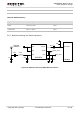


Table Of Contents
- About the Document
- Contents
- Table Index
- Figure Index
- 1 Introduction
- 2 Product Concept
- 3 Application Interface
- 3.1. General Description
- 3.2. Pin Assignment
- 3.3. Pin Description
- 3.4. Operating Modes
- 3.5. Power Saving
- 3.6. Power Supply
- 3.7. Turn on and off Scenarios
- 3.8. Reset the Module
- 3.9. RTC Backup
- 3.10. UART Interface
- 3.11. USIM Card Interface
- 3.12. USB Interface
- 3.13. PCM and I2C Interface
- 3.14. ADC Function
- 3.15. Network Status Indication
- 3.16. Operating Status Indication
- 3.17. Behavior of the RI
- 4 GNSS Receiver
- 5 Antenna Interface
- 6 Electrical, Reliability and Radio Characteristics
- 7 Mechanical Dimensions
- 8 Storage and Manufacturing
- 9 Appendix A Reference
UMTS/HSPA Module Series
UC20 Hardware Design
UC20_Hardware_Design Confidential / Released 61 / 84
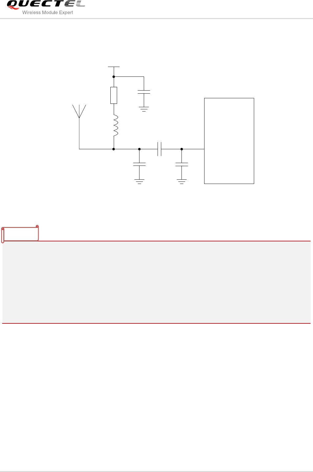
5.2.2. Reference Design for Active Antenna
Active
antenna
VDD
Module
ANT_GNSS
47nH
10R
0.1uF
100pF
NMNM
Figure 36: Reference Circuit of GNSS Active Antenna
1. You can choose the corresponding reference circuit above according to your demands on antenna
circuit design.
2. MAX2659 is the recommended LNA chip. You can disable LNA to save power with one GPIO
shown in above figure. Pay attention to this pin’s voltage level.
3. VDD supplies power for active antenna. You can choose the right VDD according to the requirements
for active antenna. This power circuit is not needed if passive antenna is applied here.
4. All NM capacitors are reserved for adjusting RF performance.
5. The capacitance of ESD component D1 should be less than 1Pf (e.g. LXES15AAA1-100).
5.3. Antenna Installation
5.3.1. Antenna Requirement
The following table shows the requirement on /UMTS antenna and GNSS antenna.
NOTES