
User's Manual
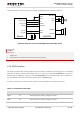
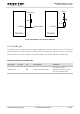


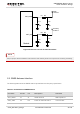
Table Of Contents
- About the Document
- Contents
- Table Index
- Figure Index
- 1 Introduction
- 2 Product Concept
- 3 Application Interface
- 3.1. General Description
- 3.2. Pin Assignment
- 3.3. Pin Description
- 3.4. Operating Modes
- 3.5. Power Saving
- 3.6. Power Supply
- 3.7. Turn on and off Scenarios
- 3.8. Reset the Module
- 3.9. RTC Backup
- 3.10. UART Interface
- 3.11. USIM Card Interface
- 3.12. USB Interface
- 3.13. PCM and I2C Interface
- 3.14. ADC Function
- 3.15. Network Status Indication
- 3.16. Operating Status Indication
- 3.17. Behavior of the RI
- 4 GNSS Receiver
- 5 Antenna Interface
- 6 Electrical, Reliability and Radio Characteristics
- 7 Mechanical Dimensions
- 8 Storage and Manufacturing
- 9 Appendix A Reference
UMTS/HSPA Module Series
UC20 Hardware Design
UC20_Hardware_Design Confidential / Released 59 / 84
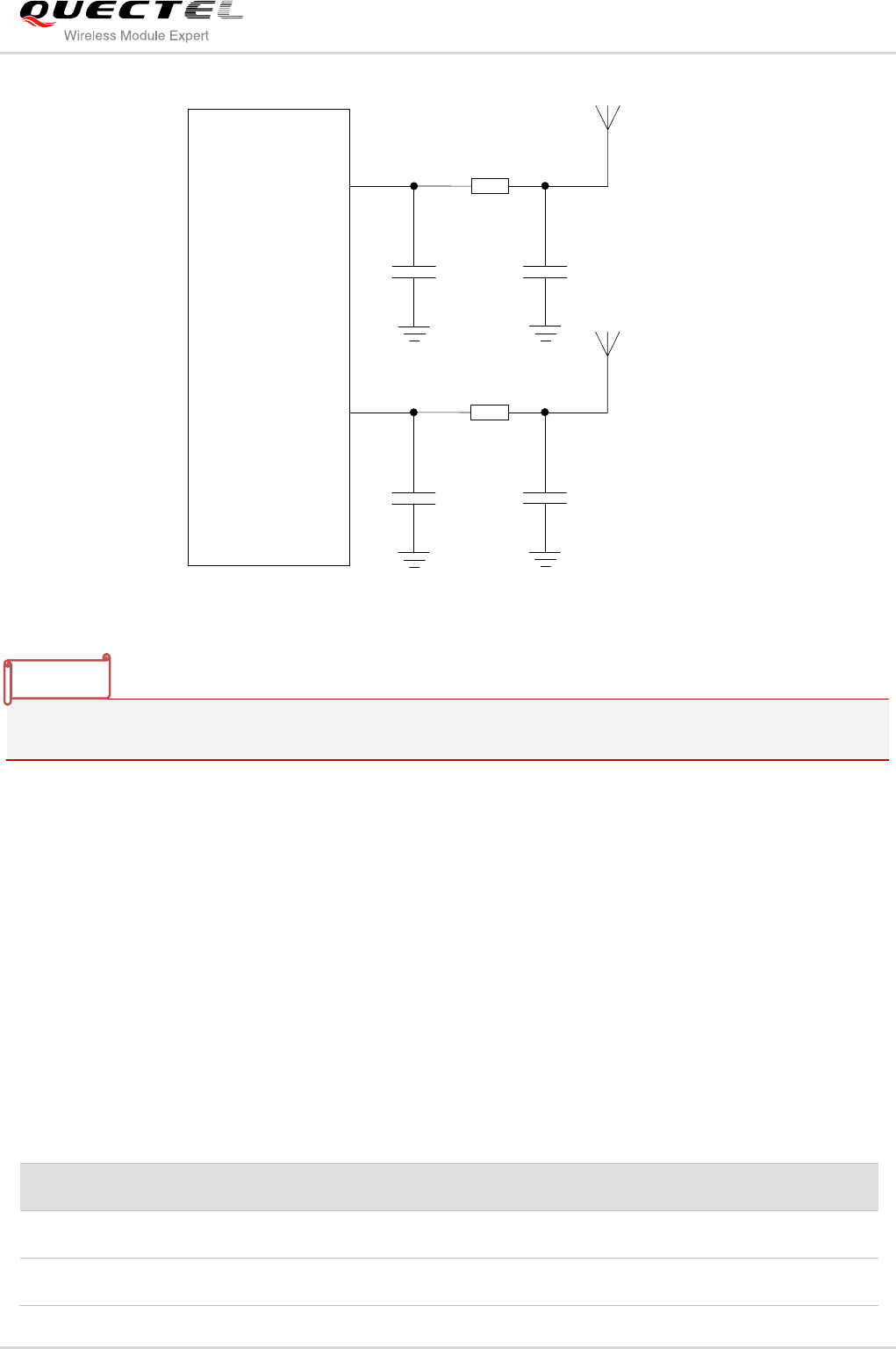
ANT_MAIN
R1 0R
C1
Module
Main
antenna
NM
C2
NM
R2 0R
C3
Diversity
antenna
NM
C4
NM
ANT_DIV
Figure 34: Reference Circuit of Antenna Interface
Keep a proper distance between main antenna and diversity antenna to improve the receiving sensitivity.
5.2. GNSS Antenna Interface
The following tables show the GNSS antenna pin definition and frequency specification.
Table 27: Pin Definition of GNSS Antenna
Pin Name
Pin No.
I/O
Description
Comment
ANT_GNSS
47
AI
GNSS antenna
50Ω impedance
VDD_2V85
34
PO
Power for external LNA or
Vnorm=2.85V
NOTE