
User's Manual
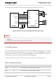
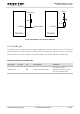


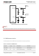
Table Of Contents
- About the Document
- Contents
- Table Index
- Figure Index
- 1 Introduction
- 2 Product Concept
- 3 Application Interface
- 3.1. General Description
- 3.2. Pin Assignment
- 3.3. Pin Description
- 3.4. Operating Modes
- 3.5. Power Saving
- 3.6. Power Supply
- 3.7. Turn on and off Scenarios
- 3.8. Reset the Module
- 3.9. RTC Backup
- 3.10. UART Interface
- 3.11. USIM Card Interface
- 3.12. USB Interface
- 3.13. PCM and I2C Interface
- 3.14. ADC Function
- 3.15. Network Status Indication
- 3.16. Operating Status Indication
- 3.17. Behavior of the RI
- 4 GNSS Receiver
- 5 Antenna Interface
- 6 Electrical, Reliability and Radio Characteristics
- 7 Mechanical Dimensions
- 8 Storage and Manufacturing
- 9 Appendix A Reference
UMTS/HSPA Module Series
UC20 Hardware Design
UC20_Hardware_Design Confidential / Released 53 / 84
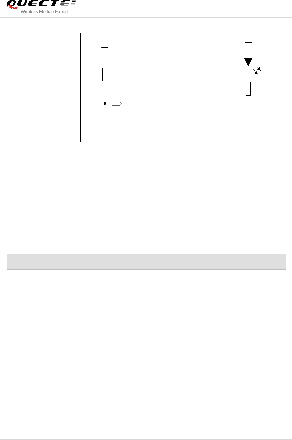
VDD_MCU
10K
Module
STATUS MCU_GPIO
Module
STATUS
VBAT
2.2K
Figure 32: Reference Circuit of the STATUS
3.16.2. SLEEP_IND
The SLEEP_IND is an indicated pin for judging whether the module is in sleep mode or not. When the
module enters into the sleep mode, the SLEEP_IND will output a logic high level. So you can use the
SLEEP_IND for low current indication. The following table shows the pin definition of SLEEP_IND.
Table 22: Pin Definition of SLEEP_IND
Pin Name
Pin No.
I/O
Description
Comment
SLEEP_IND
3
DO
Indicate the sleep status.
1.8V power domain.
Outputs high level when the
module is in sleep mode.