
User's Manual
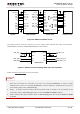
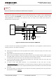
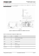
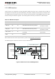
Table Of Contents
- About the Document
- Contents
- Table Index
- Figure Index
- 1 Introduction
- 2 Product Concept
- 3 Application Interface
- 3.1. General Description
- 3.2. Pin Assignment
- 3.3. Pin Description
- 3.4. Operating Modes
- 3.5. Power Saving
- 3.6. Power Supply
- 3.7. Turn on and off Scenarios
- 3.8. Reset the Module
- 3.9. RTC Backup
- 3.10. UART Interface
- 3.11. USIM Card Interface
- 3.12. USB Interface
- 3.13. PCM and I2C Interface
- 3.14. ADC Function
- 3.15. Network Status Indication
- 3.16. Operating Status Indication
- 3.17. Behavior of the RI
- 4 GNSS Receiver
- 5 Antenna Interface
- 6 Electrical, Reliability and Radio Characteristics
- 7 Mechanical Dimensions
- 8 Storage and Manufacturing
- 9 Appendix A Reference
UMTS/HSPA Module Series
UC20 Hardware Design
UC20_Hardware_Design Confidential / Released 49 / 84
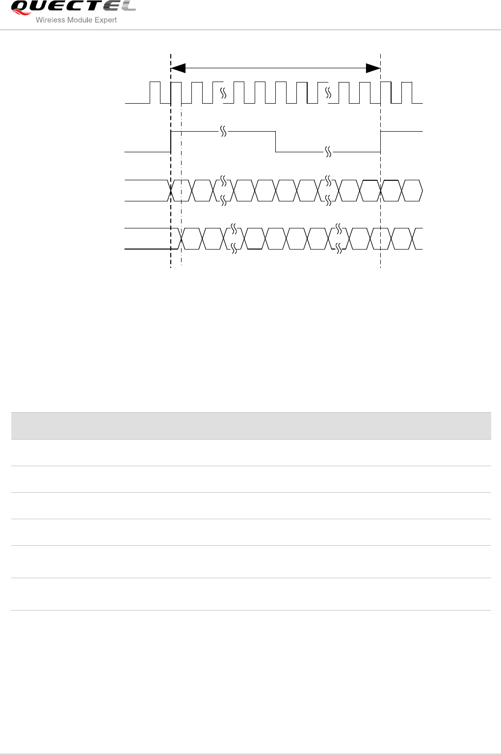
PCM_CLK
PCM_SYNC
PCM_OUT
MSB
LSB
PCM_IN
125us
MSB
1 2 1615
LSB
Figure 29: Auxiliary Mode Timing
The following table shows the pin definition of PCM and I2C interface which can be applied on audio
codec design.
Table 16: Pin Definition of PCM and I2C Interface
Pin Name
Pin No.
I/O
Description
Comment
PCM_IN
24
DI
PCM data input.
1.8V power domain.
PCM_OUT
25
DO
PCM data output.
1.8V power domain.
PCM_SYNC
26
IO
PCM data frame sync signal.
1.8V power domain.
PCM_CLK
27
IO
PCM data bit clock.
1.8V power domain.
I2C_SCL
41
DO
I2C serial clock.
Require external pull-up
resistor.
I2C_SDA
42
IO
I2C serial data.
Require external pull-up
resistor.
Clock and mode can be configured by AT command, and the default configuration is master mode using
short sync data format with 2048kHz PCM_CLK and 8kHz PCM_SYNC. In addition, UC20’s firmware has
integrated the configuration on NAU8814 application with I2C interface. Refer to document [1] about the
command AT+QDAI for details.