
User's Manual
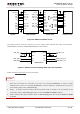
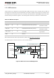
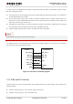
Table Of Contents
- About the Document
- Contents
- Table Index
- Figure Index
- 1 Introduction
- 2 Product Concept
- 3 Application Interface
- 3.1. General Description
- 3.2. Pin Assignment
- 3.3. Pin Description
- 3.4. Operating Modes
- 3.5. Power Saving
- 3.6. Power Supply
- 3.7. Turn on and off Scenarios
- 3.8. Reset the Module
- 3.9. RTC Backup
- 3.10. UART Interface
- 3.11. USIM Card Interface
- 3.12. USB Interface
- 3.13. PCM and I2C Interface
- 3.14. ADC Function
- 3.15. Network Status Indication
- 3.16. Operating Status Indication
- 3.17. Behavior of the RI
- 4 GNSS Receiver
- 5 Antenna Interface
- 6 Electrical, Reliability and Radio Characteristics
- 7 Mechanical Dimensions
- 8 Storage and Manufacturing
- 9 Appendix A Reference
UMTS/HSPA Module Series
UC20 Hardware Design
UC20_Hardware_Design Confidential / Released 46 / 84
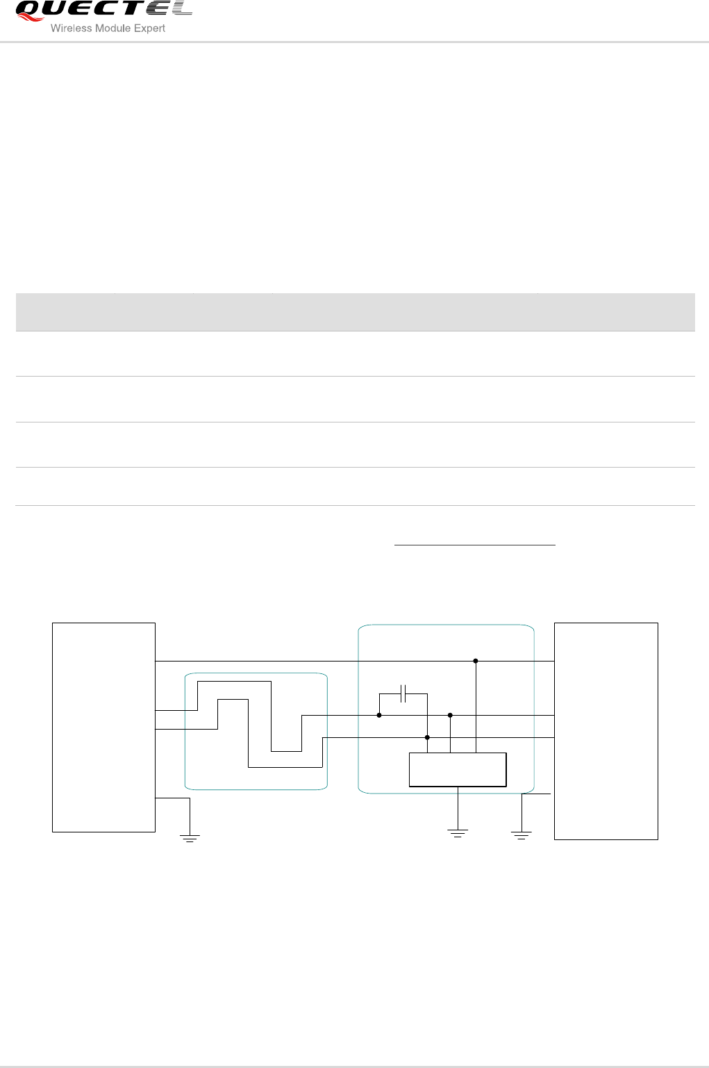
3.12. USB Interface
UC20 contains one integrated Universal Serial Bus (USB) transceiver which complies with the USB 2.0
specification and supports high speed (480 Mbps), full speed (12 Mbps) and low speed (1.5 Mbps) mode.
The USB interface is primarily used for AT command, data transmission, GNSS NMEA sentences output,
software debug and firmware upgrade. The following table shows the pin definition of USB interface.
Table 15: USB Pin Description
Pin Name
Pin No.
I/O
Description
Comment
USB_DP
69
IO
USB differential data bus (positive).
Require differential
impedance of 90Ω.
USB_DM
70
IO
USB differential data bus (minus).
Require differential
impedance of 90Ω.
USB_VBUS
71
PI
Used for detecting the USB interface
connected.
3.0~5.25V.
Typical 5.0V.
GND
72
Ground.
More details about the USB 2.0 specifications, please visit http://www.usb.org/home.
The following figure shows the reference circuit of USB interface.
Module
USB_VBUS
USB_DP
USB_DM
GND
USB connector
Close to USB connector
Differential layout
USB_VBUS
USB_DP
USB_DM
GND
ESD Array
NM_2pF
Figure 26: Reference Circuit of USB Application