
User's Manual
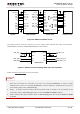
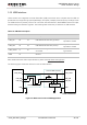
Table Of Contents
- About the Document
- Contents
- Table Index
- Figure Index
- 1 Introduction
- 2 Product Concept
- 3 Application Interface
- 3.1. General Description
- 3.2. Pin Assignment
- 3.3. Pin Description
- 3.4. Operating Modes
- 3.5. Power Saving
- 3.6. Power Supply
- 3.7. Turn on and off Scenarios
- 3.8. Reset the Module
- 3.9. RTC Backup
- 3.10. UART Interface
- 3.11. USIM Card Interface
- 3.12. USB Interface
- 3.13. PCM and I2C Interface
- 3.14. ADC Function
- 3.15. Network Status Indication
- 3.16. Operating Status Indication
- 3.17. Behavior of the RI
- 4 GNSS Receiver
- 5 Antenna Interface
- 6 Electrical, Reliability and Radio Characteristics
- 7 Mechanical Dimensions
- 8 Storage and Manufacturing
- 9 Appendix A Reference
UMTS/HSPA Module Series
UC20 Hardware Design
UC20_Hardware_Design Confidential / Released 42 / 84
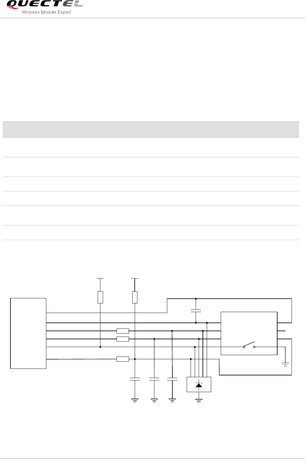
3.11. USIM Card Interface
3.11.1. USIM Card Application
The USIM card interface circuitry meets ETSI and IMT-2000 SIM interface requirements. Both 1.8V and
3.0V USIM cards are supported.
Table 12: Pin Definition of the USIM Interface
Pin Name
Pin No.
I/O
Description
Comment
USIM_VDD
14
PO
Power supply for USIM card.
Either 1.8V or 3.0V is supported by
the module automatically.
USIM_DATA
15
IO
Data signal of USIM card.
Pull-up to USIM_VDD with 15k
resistor internally.
USIM_CLK
16
DO
Clock signal of USIM card.
USIM_RST
17
DO
Reset signal of USIM card.
USIM_PRES
ENCE
13
DI
USIM card insertion detection.
1.8V power domain.
USIM_GND
10
Specified ground for USIM card.
The following figure shows the reference design of the 8-pin USIM card.
Module
USIM_VDD
USIM_GND
USIM_RST
USIM_CLK
USIM_DATA
USIM_PRESENCE
22R
22R
22R
VDD_EXT
51K
100nF USIM Connector
GND
GND
ESDA6V8AV6
33pF
33pF 33pF
VCC
RST
CLK
IO
VPP
GND
GND
USIM_VDD
15K
Figure 22: Reference Circuit of the 8 Pin USIM Card