
User's Manual
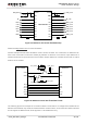
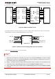
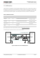
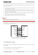
Table Of Contents
- About the Document
- Contents
- Table Index
- Figure Index
- 1 Introduction
- 2 Product Concept
- 3 Application Interface
- 3.1. General Description
- 3.2. Pin Assignment
- 3.3. Pin Description
- 3.4. Operating Modes
- 3.5. Power Saving
- 3.6. Power Supply
- 3.7. Turn on and off Scenarios
- 3.8. Reset the Module
- 3.9. RTC Backup
- 3.10. UART Interface
- 3.11. USIM Card Interface
- 3.12. USB Interface
- 3.13. PCM and I2C Interface
- 3.14. ADC Function
- 3.15. Network Status Indication
- 3.16. Operating Status Indication
- 3.17. Behavior of the RI
- 4 GNSS Receiver
- 5 Antenna Interface
- 6 Electrical, Reliability and Radio Characteristics
- 7 Mechanical Dimensions
- 8 Storage and Manufacturing
- 9 Appendix A Reference
UMTS/HSPA Module Series
UC20 Hardware Design
UC20_Hardware_Design Confidential / Released 41 / 84
TXB0108PWR
DCD_3.3V
RTS_3.3V
DTR_3.3V
RXD_3.3V
RI_3.3V
CTS_3.3V
TXD_3.3V
DCD
RTS
DTR
RXD
RI
CTS
TXD
DCD_1.8V
RTS_1.8V
DTR_1.8V
RXD_1.8V
RI_1.8V
CTS_1.8V
TXD_1.8V
VCCA
Module
GND GND
VDD_EXT VCCB
3.3V
DIN1
ROUT3
ROUT2
ROUT1
DIN4
DIN3
DIN2
DIN5
R1OUTB
FORCEON
/FORCEOFF
/INVALID
3.3V
DOUT1
DOUT2
DOUT3
DOUT4
DOUT5
RIN3
RIN2
RIN1
VCC GND
OE
SN65C3238
DB-9
Connect to PC
DCD
RTS
DTR
TXD
RI
CTS
RXD
DSR
GND
1
2
3
4
5
6
7
8
9
Figure 20: RS232 Level Match Circuit
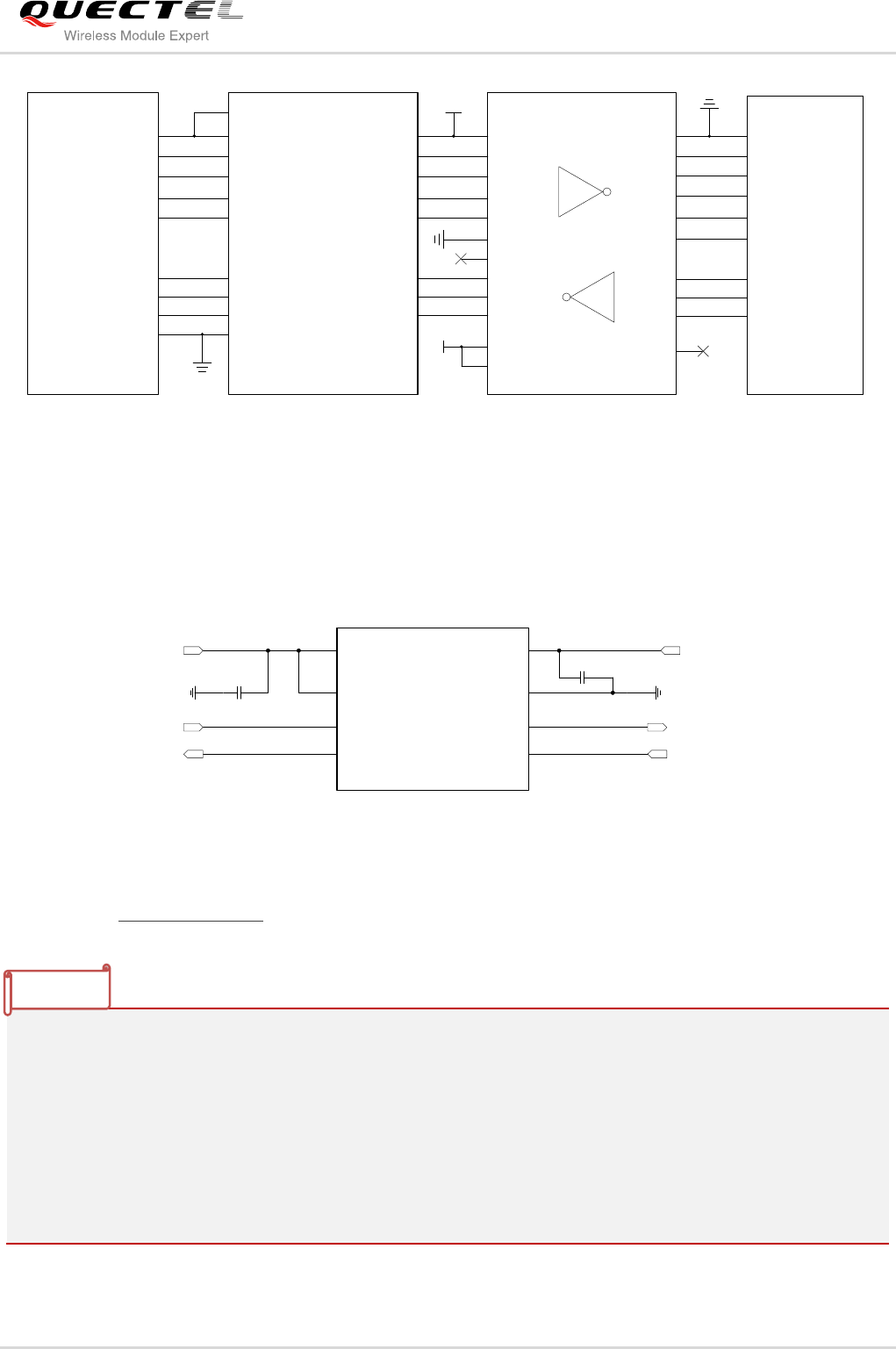
The following figure shows the reference circuit of debug UART interface with logic level translator.
TXB0102DCU provided by Texas Instruments is recommended.
VCCA VCCB
OE
A1
A2
GND
B1
B2
VDD_EXT
DBG_TXD
DBG_RXD
0.1uF
0.1uF
DBG_TXD_3.3V
DBG_RXD_3.3V
VDD_3.3V
TXB0102DCU
Figure 21: Reference Circuit of Debug UART with Level Translator
Please visit http://www.ti.com for more information.
1. The module disables the hardware flow control by default. When hardware flow control is required,
RTS and CTS should be connected to the host. AT command AT+IFC=2,2 is used to enable
hardware flow control. AT command AT+IFC=0,0 is used to disable the hardware flow control. For
more details, please refer to document [1].
2. Rising on DTR will let the module exit from the data mode by default. It can be disabled by AT
commands. Refer to document [1] about the command AT&D and AT&V for details.
3. DCD is used as data mode indication. Refer to document [1] about the command AT&C and AT&V
for details.
NOTES