
User's Manual
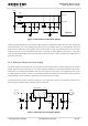

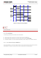

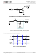
Table Of Contents
- About the Document
- Contents
- Table Index
- Figure Index
- 1 Introduction
- 2 Product Concept
- 3 Application Interface
- 3.1. General Description
- 3.2. Pin Assignment
- 3.3. Pin Description
- 3.4. Operating Modes
- 3.5. Power Saving
- 3.6. Power Supply
- 3.7. Turn on and off Scenarios
- 3.8. Reset the Module
- 3.9. RTC Backup
- 3.10. UART Interface
- 3.11. USIM Card Interface
- 3.12. USB Interface
- 3.13. PCM and I2C Interface
- 3.14. ADC Function
- 3.15. Network Status Indication
- 3.16. Operating Status Indication
- 3.17. Behavior of the RI
- 4 GNSS Receiver
- 5 Antenna Interface
- 6 Electrical, Reliability and Radio Characteristics
- 7 Mechanical Dimensions
- 8 Storage and Manufacturing
- 9 Appendix A Reference
UMTS/HSPA Module Series
UC20 Hardware Design
UC20_Hardware_Design Confidential / Released 39 / 84
DTR
66
DI
Data terminal ready.
1.8V power domain.
TXD
67
DO
Transmit data.
1.8V power domain.
RXD
68
DI
Receive data.
1.8V power domain.
Table 10: Pin Definition of the Debug UART Interface
Pin Name
Pin No.
I/O
Description
Comment
DBG_TXD
12
DO
Transmit data.
1.8V power domain.
DBG_RXD
11
DI
Receive data.
1.8V power domain.
The logic levels are described in the following table.
Table 11: Logic Levels of Digital I/O
Parameter
Min
Max
Unit
V
IL
-0.3
0.6
V
V
IH
1.2
2.0
V
V
OL
0
0.45
V
V
OH
1.35
1.8
V
UC20 provides 1.8V UART interface. A level translator should be used if your application is equipped with
a 3.3V UART interface. A level translator TXB0108PWR provided by Texas Instruments is
recommended. The following figure shows the reference design of the TXB0108PWR.