
User's Manual
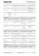
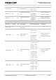
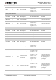
Table Of Contents
- About the Document
- Contents
- Table Index
- Figure Index
- 1 Introduction
- 2 Product Concept
- 3 Application Interface
- 3.1. General Description
- 3.2. Pin Assignment
- 3.3. Pin Description
- 3.4. Operating Modes
- 3.5. Power Saving
- 3.6. Power Supply
- 3.7. Turn on and off Scenarios
- 3.8. Reset the Module
- 3.9. RTC Backup
- 3.10. UART Interface
- 3.11. USIM Card Interface
- 3.12. USB Interface
- 3.13. PCM and I2C Interface
- 3.14. ADC Function
- 3.15. Network Status Indication
- 3.16. Operating Status Indication
- 3.17. Behavior of the RI
- 4 GNSS Receiver
- 5 Antenna Interface
- 6 Electrical, Reliability and Radio Characteristics
- 7 Mechanical Dimensions
- 8 Storage and Manufacturing
- 9 Appendix A Reference
UMTS/HSPA Module Series
UC20 Hardware Design
UC20_Hardware_Design Confidential / Released 23 / 84
RXD
68
DI
Receive data.
V
IL
min = -0.3V
V
IL
max = 0.6V
V
IH
min = 1.2V
V
IH
max = 2.0V
1.8V power domain.
Debug UART Interface
Pin Name
Pin No.
I/O
Description
DC Characteristics
Comment
DBG_TXD
12
DO
Transmit data.
V
OL
max = 0.45V
V
OH
min = 1.35V
1.8V power domain.
DBG_RXD
11
DI
Receive data.
V
IL
min = -0.3V
V
IL
max = 0.6V
V
IH
min = 1.2V
V
IH
max = 2.0V
1.8V power domain.
RF Interface
Pin Name
Pin No.
I/O
Description
DC Characteristics
Comment
ANT_DIV
35
AI
Diversity antenna.
50Ω impedance
ANT_MAIN
49
IO
Main antenna.
50Ω impedance
ANT_GNSS
47
AI
GNNS antenna.
50Ω impedance
PCM Interface
Pin Name
Pin No.
I/O
Description
DC Characteristics
Comment
PCM_IN
24
DI
PCM data input.
V
IL
min = -0.3V
V
IL
max = 0.6V
V
IH
min = 1.2V
V
IH
max = 2.0V
1.8V power domain.
PCM_OUT
25
DO
PCM data output.
V
OL
max = 0.45V
V
OH
min = 1.35V
1.8V power domain.
PCM_SYNC
26
IO
PCM data frame
sync signal.
V
OL
max = 0.45V
V
OH
min = 1.35V
V
IL
min = -0.3V
V
IL
max = 0.6V
V
IH
min = 1.2V
V
IH
max = 2.0V
1.8V power domain.
In master mode, it is
an output signal. In
slave mode, it is an
input signal.
PCM_CLK
27
IO
PCM data bit clock.
V
OL
max = 0.45V
V
OH
min = 1.35V
V
IL
min = -0.3V
V
IL
max = 0.6V
V
IH
min = 1.2V
V
IH
max = 2.0V
1.8V power domain.
In master mode, it’s
an output signal. In
slave mode, it is an
input signal.