
User's Manual
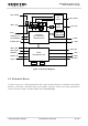
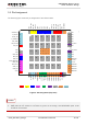
Table Of Contents
- About the Document
- Contents
- Table Index
- Figure Index
- 1 Introduction
- 2 Product Concept
- 3 Application Interface
- 3.1. General Description
- 3.2. Pin Assignment
- 3.3. Pin Description
- 3.4. Operating Modes
- 3.5. Power Saving
- 3.6. Power Supply
- 3.7. Turn on and off Scenarios
- 3.8. Reset the Module
- 3.9. RTC Backup
- 3.10. UART Interface
- 3.11. USIM Card Interface
- 3.12. USB Interface
- 3.13. PCM and I2C Interface
- 3.14. ADC Function
- 3.15. Network Status Indication
- 3.16. Operating Status Indication
- 3.17. Behavior of the RI
- 4 GNSS Receiver
- 5 Antenna Interface
- 6 Electrical, Reliability and Radio Characteristics
- 7 Mechanical Dimensions
- 8 Storage and Manufacturing
- 9 Appendix A Reference
UMTS/HSPA Module Series
UC20 Hardware Design
UC20_Hardware_Design Confidential / Released 19 / 84
3.3. Pin Description
The following tables show the UC20’s pin definition.
Table 3: IO Parameters Definition
Type
Description
IO
Bidirectional input/output
DI
Digital input
DO
Digital output
PI
Power input
PO
Power output
AI
Analog input
AO
Analog output
OD
Open drain
Table 4: Pin Description
Power Supply
Pin Name
Pin No.
I/O
Description
DC Characteristics
Comment
VBAT_BB
59,60
PI
Power supply for
module baseband
part.
Vmax = 4.3V
Vmin = 3.4V
Vnorm = 3.8V
It must be able to
provide sufficient
current up to 0.8A.
VBAT_RF
57,58
PI
Power supply for
module RF part.
Vmax = 4.3V
Vmin = 3.4V
Vnorm = 3.8V
It must be able to
provide sufficient
current in a transmitting
burst which typically
rises to 2.0A.
VRTC
18
IO
Power supply for
internal RTC circuit.
V
O
max = 3.25V
when VBAT ≥ 3.4V.
V
I
= 1.5V~3.25V at
I
IN
= 3uA when
VBAT is not applied.