
User's Manual
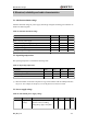

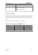
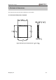
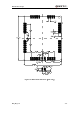


Table Of Contents
- Contents
- Table Index
- Figure Index
- 0. Revision history
- 1. Introduction
- 2. Product concept
- 3. Application interface
- 3.1. Pin
- 3.2. Operating modes
- 3.3. Power supply
- 3.4. Power on and down scenarios
- 3.5. Power saving
- 3.6. Summary of state transitions
- 3.7. RTC backup
- 3.8. Serial interfaces
- 3.9. Audio interfaces
- 3.10. SIM card interface
- 3.12. Behaviors of the RI
- 3.13. Network status indication
- 3.14. Operating status indication
- 4. Antenna interface
- 5. Electrical, reliability and radio characteristics
- 6. Mechanical dimensions
- 7. Storage and Manufacturing
- Appendix A: GPRS coding schemes
- Appendix B: GPRS multi-slot classes

M95 Hardware Design
M95_HD_V1.0 - 63 -
Voltage drop
during
transmitting
burst
Maximum power control level
on GSM850 and GSM900.
400
mV
Voltage
ripple
Maximum power control level
on GSM850 and GSM900
@ f<200kHz
@ f>200kHz
50
2
mV
mV
I
VBAT
Average
supply
current
POWER DOWN mode
SLEEP mode @ DRX=5
30
0.9
uA
mA
IDLE mode
GSM850/EGSM 900
DCS1800/PCS1900
13
13
mA
mA
TALK mode
GSM850/EGSM 900
1)
DCS1800/PCS1900
2)
206/214
153/152
mA
mA
Peak supply
current
(during
transmission
slot)
Maximum power control level
on GSM850 and GSM900.
1.5
2
A
1)
Power control level PCL 5
2)
Power control level PCL 0
5.4. Current consumption
The values of current consumption are shown in Table 27.
Table 27: The module current consumption
Condition
Current Consumption
Voice Call
GSM850
@power level #5 <300mA,Typical 206mA
@power level #12,Typical 95mA
@power level #19,Typical 73mA
GSM900
@power level #5 <300mA,Typical 214mA
@power level #12,Typical 74mA
@power level #19,Typical 73mA
DCS1800
@power level #0 <250mA,Typical 153mA
@power level #7,Typical 82mA