
User's Manual
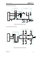
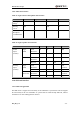
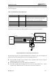
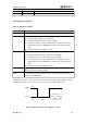
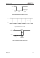
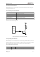
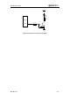

Table Of Contents
- Contents
- Table Index
- Figure Index
- 0. Revision history
- 1. Introduction
- 2. Product concept
- 3. Application interface
- 3.1. Pin
- 3.2. Operating modes
- 3.3. Power supply
- 3.4. Power on and down scenarios
- 3.5. Power saving
- 3.6. Summary of state transitions
- 3.7. RTC backup
- 3.8. Serial interfaces
- 3.9. Audio interfaces
- 3.10. SIM card interface
- 3.12. Behaviors of the RI
- 3.13. Network status indication
- 3.14. Operating status indication
- 4. Antenna interface
- 5. Electrical, reliability and radio characteristics
- 6. Mechanical dimensions
- 7. Storage and Manufacturing
- Appendix A: GPRS coding schemes
- Appendix B: GPRS multi-slot classes

M95 Hardware Design
M95_HD_V1.0 - 59 -
4. Antenna interface
The Pin 39 is the RF antenna pad. The RF interface has an impedance of 50Ω.
Table 20: Pin definition of the Antenna interface
4.1. RF reference design
The RF external circuit is recommended as below:
RF_ANT
0R
MODULE
NMNM
Figure 38: Reference circuit of RF
M95 provides an RF antenna PAD for customer’s antenna connection. The RF trace in host PCB
connected to the module RF antenna pad should be micro-strip line or other types of RF trace,
whose characteristic impendence should be close to 50Ω. M95 comes with grounding pads which
are next to the antenna pad in order to give a better grounding.
To minimize the loss on the RF trace and RF cable, take design into account carefully. It is
recommended that the insertion loss should meet the following requirements:
GSM850/EGSM900 is <1dB.
DCS1800/PCS1900 is <1.5dB.
Name
Pin
Function
GND
37
ground
GND
38
ground
RF_ANT
39
RF antenna pad
GND
40
ground