
User's Manual
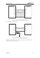
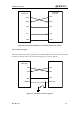
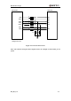
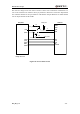
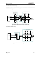
Table Of Contents
- Contents
- Table Index
- Figure Index
- 0. Revision history
- 1. Introduction
- 2. Product concept
- 3. Application interface
- 3.1. Pin
- 3.2. Operating modes
- 3.3. Power supply
- 3.4. Power on and down scenarios
- 3.5. Power saving
- 3.6. Summary of state transitions
- 3.7. RTC backup
- 3.8. Serial interfaces
- 3.9. Audio interfaces
- 3.10. SIM card interface
- 3.12. Behaviors of the RI
- 3.13. Network status indication
- 3.14. Operating status indication
- 4. Antenna interface
- 5. Electrical, reliability and radio characteristics
- 6. Mechanical dimensions
- 7. Storage and Manufacturing
- Appendix A: GPRS coding schemes
- Appendix B: GPRS multi-slot classes

M95 Hardware Design
M95_HD_V1.0 - 44 -
3.8.2. Debug Port
Debug Port
Two lines: DBG_TXD and DBG_RXD
It outputs log information automatically.
Debug Port is only used for software debugging and its baud rate must be configured as
460800bps.
Debug Computer
TXD
RXD
GND
Module(DCE)
Debug port
DBG_TXD
DBG_RXD
GND
Figure 22: Connection of software debug
3.8.3. UART Application
The reference design of 3.3V level match is shown as below. 1K and 5.6K resistors among the
following diagram are used to decrease the output voltage of MCU/ARM.