
User's Manual
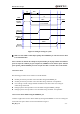
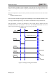


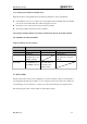
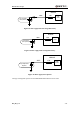
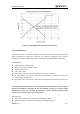
Table Of Contents
- Contents
- Table Index
- Figure Index
- 0. Revision history
- 1. Introduction
- 2. Product concept
- 3. Application interface
- 3.1. Pin
- 3.2. Operating modes
- 3.3. Power supply
- 3.4. Power on and down scenarios
- 3.5. Power saving
- 3.6. Summary of state transitions
- 3.7. RTC backup
- 3.8. Serial interfaces
- 3.9. Audio interfaces
- 3.10. SIM card interface
- 3.12. Behaviors of the RI
- 3.13. Network status indication
- 3.14. Operating status indication
- 4. Antenna interface
- 5. Electrical, reliability and radio characteristics
- 6. Mechanical dimensions
- 7. Storage and Manufacturing
- Appendix A: GPRS coding schemes
- Appendix B: GPRS multi-slot classes

M95 Hardware Design
M95_HD_V1.0 - 39 -
Figure 17: Seiko XH414H-IV01E Charge Characteristics
3.8. Serial interfaces
The module provides two serial ports: UART and Debug Port. The module is designed as a DCE
(Data Communication Equipment), following the traditional DCE-DTE (Data Terminal
Equipment) connection. Autobauding function supports baud rate from 4800bps to 115200bps.
The UART Port:
TXD: Send data to RXD of DTE
RXD: Receive data from TXD of DTE
RTS: Requests to send
CTS: Clear to send
DTR: DTE is ready and inform DCE (this pin can wake the module up)
RI: Ring indicator (when the call, SMS, data of the module are coming, the module will
output signal to inform DTE)
DCD: Data carrier detection (the valid of this pin demonstrates the communication link is set
up)
The module disables hardware flow control in default. When hardware flow control is required,
RTS and CTS should be connected to the host. AT command “AT+IFC=2,2” is used to enable
hardware flow control. AT command “AT+IFC=0,0” is used to disable the hardware flow
control. For more details, please refer to document [1].
The Debug Port
DBG_TXD: Send data to the COM port of a debugging computer
DBG_RXD: Receive data from the COM port of a debugging computer