
User's Manual

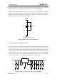
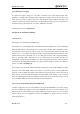
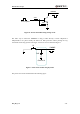
Table Of Contents
- Contents
- Table Index
- Figure Index
- 0. Revision history
- 1. Introduction
- 2. Product concept
- 3. Application interface
- 3.1. Pin
- 3.2. Operating modes
- 3.3. Power supply
- 3.4. Power on and down scenarios
- 3.5. Power saving
- 3.6. Summary of state transitions
- 3.7. RTC backup
- 3.8. Serial interfaces
- 3.9. Audio interfaces
- 3.10. SIM card interface
- 3.12. Behaviors of the RI
- 3.13. Network status indication
- 3.14. Operating status indication
- 4. Antenna interface
- 5. Electrical, reliability and radio characteristics
- 6. Mechanical dimensions
- 7. Storage and Manufacturing
- Appendix A: GPRS coding schemes
- Appendix B: GPRS multi-slot classes

M95 Hardware Design
M95_HD_V1.0 - 28 -
(0.1µF to 1µF) ceramic capacitor should be in parallel with the 100µF capacitor, which is
illustrated in Figure 4. The capacitors should be placed close to the M95 VBAT pins.
The PCB traces from the VBAT pads to the power source must be wide enough to ensure that
there is not too much voltage drop occurring in the transmitting burst mode. The width of trace
should be no less than 2mm and the principle of the VBAT trace is the longer, the wider. The
VBAT voltage drop can be measured by oscilloscope.
C2C1
VBAT
+
C1=100uF, C2=0.1uF~1uF
Figure 4: Reference circuit of the VBAT input
3.3.3. Reference power design for the module
The power design for the module is very important and the circuit design of the power supply for
the module largely depends on the power source. Figure 5 shows a reference design of +5V input
power source. The part number of this LDO IC is MIC29302WU. The designed output for the
power supply is 4.16V and the maximum load current is 3A, in order to prevent outputting
abnormal voltage, a zener voltage regulator is employed at the point of the output nearby the pin
of VBAT. Some elements have to be taken into account in the component select, such as reserve
zener voltage is recommend 5.1V and the total dissipation is more than 1Watt.
C1
100uF
C2
MIC29032 U1
IN OUT
EN
GND
ADJ
2 4
1
3
5
DC_IN VBAT
100nF
C3
100uF
C4
100nF
C5 C6
33pF
R1
10pF
D1
120K
51K
R2
5.1V
Figure 5: Reference circuit of the source power supply input