
User's Manual
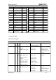
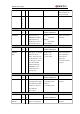
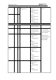
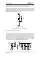
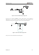
Table Of Contents
- Contents
- Table Index
- Figure Index
- 0. Revision history
- 1. Introduction
- 2. Product concept
- 3. Application interface
- 3.1. Pin
- 3.2. Operating modes
- 3.3. Power supply
- 3.4. Power on and down scenarios
- 3.5. Power saving
- 3.6. Summary of state transitions
- 3.7. RTC backup
- 3.8. Serial interfaces
- 3.9. Audio interfaces
- 3.10. SIM card interface
- 3.12. Behaviors of the RI
- 3.13. Network status indication
- 3.14. Operating status indication
- 4. Antenna interface
- 5. Electrical, reliability and radio characteristics
- 6. Mechanical dimensions
- 7. Storage and Manufacturing
- Appendix A: GPRS coding schemes
- Appendix B: GPRS multi-slot classes

M95 Hardware Design
M95_HD_V1.0 - 24 -
DBG_RXD
14
I
UART interface for
debugging only.
VILmin=-0.3V
VILmax=
0.25*VDD_EXT
VIHmin=
0.75*VDD_EXT
VIHmax=
VDD_EXT+0.3V
VOHmin=
0.85*VDD_EXT
VOLmax=
0.15*VDD_EXT
If unused, keep these
pins open.
DBG_TXD
15
O
SIM interface
PIN NAME
PIN
NO.
I/
O
DESCRIPTION
DC
CHARACTERISTICS
COMMENT
SIM_ VDD
27
O
Power supply for SIM
card
The voltage can be
selected by software
automatically. Either
1.8V or 3V.
1. All signals of SIM
interface should be
protected against ESD
with a TVS diode
array.
2. Maximum trace
length is 200mm from
the module pad to
SIM card holder.
SIM_RST
28
O
SIM reset
3V:
VOLmax=0.36V
VOHmin=
0.9*SIM_VDD
1.8V:
VOLmax=
0.2*SIM_VDD
VOHmin=
0.9*SIM_VDD
SIM_
DATA
29
I/
O
SIM data
3V:
VOLmax=0.4V
VOHmin=
SIM_VDD-0.4V
1.8V:
VOLmax=
0.15*SIM_VDD
VOHmin=
SIM1_VDD-0.4V
SIM_CLK
30
O
SIM clock
3V:
VOLmax=0.4V
VOHmin=
0.9*SIM_VDD
1.8V:
VOLmax=
0.12*SIM_VDD