
User`s guide


Chapter 2
29
KEMF-4010 User’s
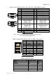
Table 33 LVDS1, LVDS Panel Connector
Signal Name Pin Pin Signal Name
NC 2 1 NC
+3.3V / +5V* 4 3 +3.3V / +5V*
TxclkB- 6 5 TxclkA-
TxclkB+ 8 7 TxclkA+
GND 10 9 GND
TxoutB0- 12 11 TxoutA0-
TxoutB0+ 14 13 TxoutA0+
TxoutB1- 16 15 TxoutA1-
TxoutB1+ 18 17 TxoutA1+
TxoutB2- 20 19 TxoutA2-
TxoutB2+ 22 21 TxoutA2+
TxoutB3- 24 23 TxoutA3-
TxoutB3+ 26 25 TxoutA3+
GND 28 27 GND
I2C_Clock 30 29 I2C_Data
Pitch: 1.25mm Tin Plated [HIROSE DF13-30DP-1.25(24)]
Cable: 0C5029003000070L LVDS Port cable, 30-pin 1.25mm to DVI connector with bracket, L=30cm
* The voltage is selected by JP11
Note: If DVI cable is connecting to LVDS panel connector, the JP11 Pin2-3 should be shorted.
Table 34 IR1, IrDA Pin Header
Pin Signal Name
1 +5V
2 Key
3 RXD
4 GND
5 TXD
Pitch: 2.54mm [YIMTEX 3321*05SAGR-02]
Table 35 PCI1, 32-bit / 33Mhz / 5V-key PCI Slot
Pin Side B Side A
1 -12V Reserved
2 Reserved +12V
3 Ground Reserved
4 Reserved Reserved
5+5V +5V
6+5V INTA#
7INTB# INTC#
8 INTD# +5V
9 Reserved GNT1# *
10 REQ1# * +5V