
Manual


TECHNICAL NOTES
TECHNICAL NOTESTECHNICAL NOTES
TECHNICAL NOTES
www.qtech.co.nzTel033663713
TECHNICAL NOTES
TECHNICAL NOTESTECHNICAL NOTES
TECHNICAL NOTES
ThissectiondescribesthetechnicalaspectsofQ80Modulepowersupplyandmodeminterface.
Power Supply
Power SupplyPower Supply
Power Supply
The Q80Moduleis designed tooperate withaDC powersupplyvoltage of nominally12 volt. The Q80 Module
drawsapproximately80mAinStandby,100mAonReceiveand1.2AonTransmitat5Wattsoutput.
The DC power supply to the Q80 Module must be adequately smoothed and be free from noise and voltage
transients.WheretheDCsupplyisderivedfromtheACmains,orbatterieswithanassociatedACmainsbattery
chargerthesedevicesmustcomplywiththerequiredelectricalregulations.
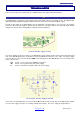
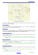
LocationofPowersupplycircuitry.
The above diagramshowsthelocation of the Q80 Module powersupplycircuit located at thebottom right hand
side of the Q80 Motherboard as view with the front panel BNC RF connector to the right. The power supply
connectorP1isa3wayconnectorlabelled‘PWR’onthebottompaneloftheQ80Module.Theconnectionstothe
powerconnectorare:
CTL PinNo1-TheremotepowerON/OFFcontrolinput.
+IN PinNo2-Thepositiveleadofthepowersupply.
G PinNo3-Ground,thenegativeleadofthepowersupply.
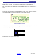
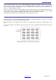
CircuitdetailsofPowerSupplyFrontEnd.
Inthe abovecircuitdiagram the15 volt zener diodeD1and the 2 ampfuseF1 protect theQ80 moduleagainst
reversepowersupplyconnection,overvoltageandtransientvoltages.Thefuseisaplug-in2ampTE5fuse.