
Technical data

USB and PS/2 Multimedia Keyboard Interface
USB and PS/2 Multimedia Keyboard Interface, Rev. 1
12 Freescale Semiconductor
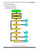
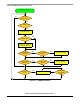
1.5.1 USB and PS/2 Detection
PTE3 and PTE4 can be configured as USB D+ and D– pins or as open-drain I/O pins for PS/2 data and
clock lines.
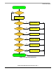
Figure 1-7 shows the algorithm for distinguishing between a USB and a PS/2 interface.
After power on, the interface protocol is undetermined and can be either a USB or a PS/2 interface. The
firmware first initializes the registers and the I/O ports. It then performs a 350ms software delay to meet
the PS/2 power on delay requirement. The USB engine and the internal USB pullup resistor are enabled.
PTE3 and PTE4 are configured as USB D+ and D– pins with a 1.5K internal pullup at D– pin.
For a low speed USB interface, D+ pin will not be continuously high for more than 4µs because of the bit
stuffing mechanism. The PS/2 interface is determined by 1ms continuously high at D+ pin while the USB
interface is determined by receiving a SETUP token.
After the interface mode is detected. the firmware enters either the PS/2 or USB main routine.
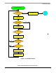
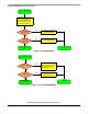
1.5.2 PS/2 Main Routine
In PS/2 mode, PTE3 and PTE4 are configured as open-drain I/O pins with 5K internal pullup resistors
enabled.
Figure 1-8 shows the PS/2 main routine. The main functions of the PS/2 routines are:
• Receive commands from host
• Respond to received commands
• Scan key matrix
• Send make code to host if key pressed
• Send break code to host if key released
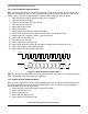
1.5.3 PS/2 Protocol
The PS/2 is a bidirectional serial interface using two signals: Clock and Data. The data consists of 11 bits
including 1 start bit, 8 data bits, 1 odd parity bit, and 1 stop bit. PS/2 device generates the clock signal
with a typical cycle of 80µs in both host-to-device or device-to-host communications.
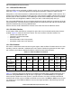
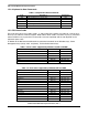
Table 1-1. Clock and Data Line Control
Register Bits Port Pins
Register POCR PTE DDRE IOCR POCR PTE DDRE
PTE4
(Data)
PTE3
(Clock)
Bit PTE4P PTE4 DDRE4 PTE4IE PTE3P PTE3 DDRE3
PTE4
(Data)
PTE3
(Clock)
PTE4 Interrupt
Enabled
— — — 1 — — —
Input
High
—
Release
Data/Clock High
1 — 0 — 1 — 0
Input
High
Input
High
Drive
Data/Clock Low
— 0 1 — — 0 1
Output
Low
Output
Low
Table 1-1 shows the setting of the registers for controlling the PTE3 (Clock) and the PTE4 (Data) pins.
Instead of setting DDR3/DDR4 as high to output a high signal, we set DDR3/DDR4 as an input with
internal pullup to perform the same function. In the PS/2 routines, the values of PTE3 and PTE4 are
cleared to zero and the values of PTE3P and PTE4P are set to one. Set DDR3 or DDR4 to one to force
it as output low, or clear DDR3 or DDR4 to zero to make it high impedance and pulled high by the 5K
internal resistor.