USB and PS/2 Multimedia Keyboard Interface Designer Reference Manual M68HC08 Microcontrollers DRM014 Rev. 1 4/2006 freescale.
USB and PS/2 Multimedia Keyboard Interface Designer Reference Manual by: Derek Lau Freescale Semiconductor, Inc. Hong Kong To provide the most up-to-date information, the revision of our documents on the World Wide Web will be the most current. Your printed copy may be an earlier revision. To verify that you have the latest information available, refer to http://www.freescale.com The following revision history table summarizes changes contained in this document.
Revision History USB and PS/2 Multimedia Keyboard Interface, Rev. 1.
Table of Contents Chapter 1 USB and PS/2 Multimedia Keyboard Interface 1.1 1.2 1.3 1.4 1.4.1 1.4.2 1.5 1.5.1 1.5.2 1.5.3 1.5.4 1.5.5 1.5.6 1.5.7 1.5.8 1.5.9 1.5.10 1.6 1.7 1.8 1.8.1 1.8.2 1.9 1.10 1.10.1 1.11 Introduction . . . . . . . . . . . . . . . . . . . . . . . . . . . . . . . . . . . . . . . . . . . . . . . . . . . . . . . . . . . . . . . . . 7 Overview . . . . . . . . . . . . . . . . . . . . . . . . . . . . . . . . . . . . . . . . . . . . . . . . . . . . . . . . . . . . . . . . . . .
Table of Contents USB and PS/2 Multimedia Keyboard Interface 6 Freescale Semiconductor
Chapter 1 USB and PS/2 Multimedia Keyboard Interface 1.1 Introduction This manual describes a reference design of a Universal Serial Bus and PS/2 multimedia keyboard interface for Microsoft Windows by using the MC68HC908JB8. For the full MC68HC908JB8 specification, please refer to the data sheet, Freescale order number: MC68HC908JB8/D. 1.2 Overview The Freescale MC68HC908JB8 is a member of the HC08 Family of microcontrollers (MCUs).
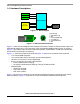
USB and PS/2 Multimedia Keyboard Interface 1.4 Hardware Descriptions Scroll LED Caps LED Num LED MC68HC908JB8 8 x 18 Key Matrix USB Plug Figure 1-1. . Block Diagram 6 5 USB Plug USB to PS/2 Converter 3 1 2 4 PS/2 Plug 6-pin PS/2 Plug 1 – Data (USB D– pin) 2 – NC 3 – Ground (USB Ground) 4 – +5V (USB +5V) 5 – Clock (USB D+ pin) 6 – NC Figure 1-2. USB and PS/2 Connections Figure 1-1 shows the block diagram of the keyboard.
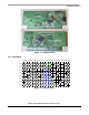
Hardware Descriptions Figure 1-3. Keyboard PCB 1.4.1 Key Matrix PTB0 PTB1 PTB2 PTB3 PTB4 PTB5 PTB6 PTB7 PTC0 PTC1 PTC2 PTC3 PTC4 PTC5 PTC6 PTC7 PTE0 PTE2 PTA0 End 9 8 7 4 3 2 1 Page PWR SLEEP Down Dwn PTA1 Home F8 + = 6 5 F2 F1 ~ ` Page Up N B < , M V C F6 H G F4 L K J F D F7 ]} Y T O I U R PTA2 App PTA3 > . PTA4 PTA5 ENT PTA6 PTA7 + INS Prnt Scr DEL F5 0 F10 Lctrl _ - F9 ? / F12 RALT Z * / Num Lck ESC .
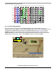
USB and PS/2 Multimedia Keyboard Interface PTB0 PTB1 PTB2 PTB3 PTB4 PTB5 PTB6 PTB7 PTC0 PTC1 PTC2 PTC3 PTC4 PTC5 PTC6 PTC7 PTE0 PTE2 PTA0 J 7 1 LCTRL MK7 MK5 MK2 7 JPN3 F4 Z Q ESC Fn 5 _ - PTA1 K 8 2 MK0 MK8 LGUI 8 INS F5 X W F1 MK3 T + = PTA2 L 9 3 MK6 LSFT MK9 9 DEL F6 C E F2 SLEEP Q Bck Spc PTA3 ;: * + MK1 RSFT MK18 0 Num Lck F7 V R F3 MK8 B [{ PTA4 ENT 4 ENT Home RCTRL MK4 MK23 MK10 U $64 | \ F8 A 1 ~ ` Caps Lck 6 ]} PTA5 M 5 0
Firmware Description 1.5 Firmware Description The firmware consists of three main parts: • USB and PS/2 interface detection • PS/2 main program and subroutines • USB main program and subroutines INITIALIZATION DELAY 350ms (POWER ON DELAY) ENABLE USB D– PULLUP D+ HIGH FOR 1ms ? YES PS/2 NO OVER 10 SECONDS ? YES USB NO NO USB RESET? YES YES D+ HIGH FOR 1ms ? PS/2 NO SETUP DETECTED ? YES USB NO NO OVER 10 SECONDS ? YES USB Figure 1-7.
USB and PS/2 Multimedia Keyboard Interface 1.5.1 USB and PS/2 Detection PTE3 and PTE4 can be configured as USB D+ and D– pins or as open-drain I/O pins for PS/2 data and clock lines. Figure 1-7 shows the algorithm for distinguishing between a USB and a PS/2 interface. After power on, the interface protocol is undetermined and can be either a USB or a PS/2 interface. The firmware first initializes the registers and the I/O ports.
Firmware Description PS/2 INITIALIZATION NO SELF TEST PASS ? SEND SELF TEST FAIL CODE ($FC) STOP YES SEND SELF TEST PASS CODE ($AA) VALID COMMAND FROM HOST ? NO YES ACK AND HANDLE COMMAND 40ms TIMER TICK ? YES SCAN KEY MATRIX NO KEYS PRESSED OR RELEASED YES YES GHOST KEY ? NO SEND MAKE CODES FOR KEYS PRESSED SEND BREAK CODES FOR KEYS RELEASED Figure 1-8. PS/2 Main Routine USB and PS/2 Multimedia Keyboard Interface, Rev.
USB and PS/2 Multimedia Keyboard Interface 1.5.4 Host to Device Communications Data sent from host to device is read while the clock line is high. In an idle state, both the Clock and the Data lines are pulled high. The host starts sending data by pulling the Clock line low for a minimum of 100 ms. Figure 1-9 shows the signal diagram. Communications steps are shown as below: 1. Host waits until no auxiliary device transmission is in progress. 2. Host pulls the Clock line low. 3.
Firmware Description 6. Device reads the Clock line and aborts communication if the Clock line is low. 7. Repeat steps 4 to 6 for Data 0 to Data 7, the parity bit and the stop bit. 8. Device releases the Clock line high. 5,6 STEP 1,2 CLOCK 4 8 7 DATA 3 START DATA0 DATA1 DATA2 DATA3 DATA4 DATA5 DATA6 DATA7 PARITY STOP Figure 1-10. Device to Host Communication KBD_OUT is the routine for transmitting data to the host. The data to be transmitted is put into V_TxByte before calling this routine. 1.5.
USB and PS/2 Multimedia Keyboard Interface 1.5.8 Keyboard to Host Commands Table 1-3. Keyboard to Host Commands Code Description Implemented $00 Keyboard detection or overrun error YES $AA Basic assurance test passed YES $EE Echo YES $FA Acknowledge YES $FE Resend YES 1.5.9 PS/2 Scan Codes There are three sets of scan codes (code 1, 2, and 3). Most PCs support scan code set 2, hence this is the only scan code the firmware supports.
Firmware Description Table 1-6. Scan codes supported by Windows ME Make Code Break Code AC Calculator Description $E0, $2B $E0, $F0, $2B AC Local Browser $E0, $40 $E0, $F0, $40 AC Consumer Control Configuration $E0, $50 $E0, $F0, $50 1.5.10 USB Main Routine Figure 1-11 shows the USB main routine. The routine scans the keyboard every 40 ms. If there are keys pressed or released, it puts the key codes into a buffer and prepares the input reports for the keys through endpoint 1 or endpoint 2.
USB and PS/2 Multimedia Keyboard Interface USB INITIALIZATION NO DEVICE CONFIGURED ? YES 40ms TIMER TICK ? YES SCAN KEY MATRIX YES GHOST KEY? NO CONVERT SCAN KEY TO KEYBOARD REPORT YES YES EP1 TX BUFFER EMPTY ? NEW ENDPOINT 1 REPORT ? TX EP1 IN REPORT NO YES YES EP2 TX BUFFER EMPTY ? NEW ENDPOINT 2 REPORT ? TX EP2 IN REPORT NO NO YES USB IDLE FOR 6 ms ? SUSPEND DEVICE KEY PRESSED OR RESUME FROM HOST ? YES Figure 1-11. USB Main Routine USB and PS/2 Multimedia Keyboard Interface, Rev.
Firmware Description USB INTERRUPT ROUTINE NO EOP ? YES RESET SUSPEND COUNTER YES SETUP ? SETUP HANDLER NO OUT TOKEN TO EP0 ? YES OUT EP0 HANDLER NO EP0 TX COMPLETED ? YES IN EP0 HANDLER NO EP1 TX COMPLETED ? YES DISABLE EP1 TRANSMIT & CLEAR EP1 TX FLAG YES DISABLE EP2 TRANSMIT & CLEAR EP2 TX FLAG NO EP2 TX COMPLETED ? NO RESUME FORM HOST? YES CLEAR RESUME FLAG NO RETURN FROM INTERRUPT Figure 1-12. USB Interrupt Routine USB and PS/2 Multimedia Keyboard Interface, Rev.
USB and PS/2 Multimedia Keyboard Interface SETUP HANDLER 1.UNSTALL EP 0 IN & OUT 2.COPY 8 BYTE SETUP DATA TO RAM BUFFER 3.CLEAR EP0 RX FLAG 4.SET NAK TO IN EP0 STANDARD DEVICE REQUEST ? YES HANDLE STANDARD DEVICE REQUEST YES HANDLE HID CLASSE REQUEST NO HID CLASS REQUEST ? NO RETURN RETURN STALL Figure 1-13. Setup Routine OUT EP0 HANDLER STATUS STAGE ? YES 1. SET NAK TO EP0 IN 2. SET STALL TO EP0 OUT (CONTROL TRANSFER COMPLETED) NO VALID DATA YES 1. COPY DATA TO BUFFER 2.
Firmware Description IN EPO HANDLER SET NAK TO IN EP0 SET STALL TO EP0 OUT (CONTROL TRANSFER COMPLETED) YES STATUS STAGE ? NO [DATA STAGE] YES ALL DATA SENT? PREPARE FOR OUT STAGE NO PREPARE FOR NEXT DATA STAGE RETURN Figure 1-15. . IN EPO HANDLER USB Key Codes The key codes or usage IDs for a basic 104 keyboard are defined in the USB HID Usage Tables.
USB and PS/2 Multimedia Keyboard Interface Table 1-8.
Firmware Description Table 1-10. Interface 0 Output Report Byte Bit 7 Bit 6 Bit 5 0 Bit 4 Kana Bit 3 Bit 2 Bit 1 Bit 0 Compose Scroll Lock Caps Lock Num Lock Interface 1 issues power management key or multimedia key input reports, which are distinguished by a unique Report ID. The power management key uses Report ID number 1 and the multimedia key uses Report ID number 2 (see Table 1-11 and Table 1-12). Table 1-11.
USB and PS/2 Multimedia Keyboard Interface 1.6 Firmware Files Firmware is compiled under CASM08Z.EXE ver 3.16 from P & E Microcomputer Systems, Inc. Table 1-14 summarizes the functions of each firmware files: Table 1-14. Input Report Examples Files Functions JB8-PSU.ASM Define constants and variables USB and PS/2 detection PS/2 main program PS/2 key handler PS2-SCAN.ASM PS/2 key scan PS2-KEY.ASM PS/2 key matrix definition JB8-USB.
Extra Features 1.8.2 Firmware • • • • Modify the key matrix tables in "ps2-key.asm" and "usb-key.asm" according to customized key matrix layout Change vendor ID, product ID and product revision number in the device descriptor table in "usb-key.h" Change vendor name and product name in the string descriptor table in "usb-key.h" Change the report descriptor in "usb-key.h" if necessary. 1.9 Extra Features 1.10 Further Information 1.10.
USB and PS/2 Multimedia Keyboard Interface Figure 1-16. Keyboard Schematics USB and PS/2 Multimedia Keyboard Interface, Rev.
Appendix A. Glossary A — See “accumulator (A).” accumulator (A) — An 8-bit general-purpose register in the CPU08. The CPU08 uses the accumulator to hold operands and results of arithmetic and logic operations. acquisition mode — A mode of PLL operation during startup before the PLL locks on a frequency. Also see "tracking mode." address bus — The set of wires that the CPU or DMA uses to read and write memory locations. addressing mode — The way that the CPU determines the operand address for an instruction.
bus — A set of wires that transfers logic signals. bus clock — The bus clock is derived from the CGMOUT output from the CGM. The bus clock frequency, fop, is equal to the frequency of the oscillator output, CGMXCLK, divided by four. byte — A set of eight bits. C — The carry/borrow bit in the condition code register. The CPU08 sets the carry/borrow bit when an addition operation produces a carry out of bit 7 of the accumulator or when a subtraction operation requires a borrow.
CPU registers — Memory locations that are wired directly into the CPU logic instead of being part of the addressable memory map. The CPU always has direct access to the information in these registers.
binary-coded decimal arithmetic operations. The decimal adjust accumulator (DAA) instruction uses the state of the H and C bits to determine the appropriate correction factor. hexadecimal — Base 16 numbering system that uses the digits 0 through 9 and the letters A through F. high byte — The most significant eight bits of a word. illegal address — An address not within the memory map illegal opcode — A nonexistent opcode. I — The interrupt mask bit in the condition code register of the CPU08.
mask — 1. A logic circuit that forces a bit or group of bits to a desired state. 2. A photomask used in integrated circuit fabrication to transfer an image onto silicon. mask option — A optional microcontroller feature that the customer chooses to enable or disable. mask option register (MOR) — An EPROM location containing bits that enable or disable certain MCU features. MCU — Microcontroller unit. See “microcontroller.
parity — An error-checking scheme that counts the number of logic 1s in each byte transmitted. In a system that uses odd parity, every byte is expected to have an odd number of logic 1s. In an even parity system, every byte should have an even number of logic 1s. In the transmitter, a parity generator appends an extra bit to each byte to make the number of logic 1s odd for odd parity or even for even parity. A parity checker in the receiver counts the number of logic 1s in each byte.
reserved memory location — A memory location that is used only in special factory test modes. Writing to a reserved location has no effect. Reading a reserved location returns an unpredictable value. reset — To force a device to a known condition. ROM — Read-only memory. A type of memory that can be read but cannot be changed (written). The contents of ROM must be specified before manufacturing the MCU. SCI — See "serial communication interface module (SCI).
toggle — To change the state of an output from a logic 0 to a logic 1 or from a logic 1 to a logic 0. tracking mode — Mode of low-jitter PLL operation during which the PLL is locked on a frequency. Also see "acquisition mode." two’s complement — A means of performing binary subtraction using addition techniques. The most significant bit of a two’s complement number indicates the sign of the number (1 indicates negative).
How to Reach Us: Home Page: www.freescale.com E-mail: support@freescale.com USA/Europe or Locations Not Listed: Freescale Semiconductor Technical Information Center, CH370 1300 N. Alma School Road Chandler, Arizona 85224 +1-800-521-6274 or +1-480-768-2130 support@freescale.