
Data Sheet
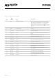
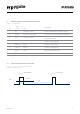


Table Of Contents
- 1PYGATE main
- PYGATE p.02 Content
- PYGATE p.03
- PYGATE p.04
- PYGATE p.05
- PYGATE p.06
- PYGATE p.07
- PYGATE p.08
- PYGATE p.09
- PYGATE p.10
- PYGATE p.11
- PYGATE p.12
- PYGATE p.13
- PYGATE p.14
- PYGATE p.15
- PYGATE p.16
- PYGATE p.17
- PYGATE p.18
- PYGATE p.19
- PYGATE p.20
- PYGATE p.21
- PYGATE p.22
- PYGATE p.23
- PYGATE p.24
- PYGATE p.25
- PYGATE p.26
- PYGATE p.27
- PYGATE p.28

12
Version 1.1
y
g
ate
go invent
6.4 POWER and UART from/to the Module header pinout
Table 6 - J6 header pins
6.5 Synchronization signal from a GPS receiver
UTC 12:00:00m UTC 12:00:01
100 mS
PPS
1 Sec
Pin
Pin
Figure 7 – 1 pulse-per-second synchronization
signal from a
GPS receiver
Type
Name
Description
1 VCC
Power Out (+VCC)
VCC is combined power from three sources, USB,
Power-over-Ethernet or Lithium battery.
+3.3V coming form voltage regulator
supplied by VCC_RF
+3.3V power coming from the Pycom
module voltage regulator
Power Out (+VCC_RF)
Power Out (+VCC_MOD)
Input
2 VCC_RF VCC power controlled by RFPWR_EN signal
Power Out (+3V3)
3 +3V3
4 3V3_MOD
5 UART_RX
6 UART_TX Output
See J5 pin 2 description
See J5 pin 3 description
*Optional 1 pulse-per-second synchronization
signal from a GPS receiver.
Ground
Input
Power (GND)
7 GPS_IN
8 GND