
Data Sheet
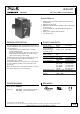

UF20.241
UF
-Series
24V, 20A, 200MS, BUFFER MODULE
Oct. 2016 / Rev. 2.0 DS-UF20.241-EN
All parameters are specified at 24V, 20A, 25°C ambient and after a 5 minutes run-in time unless otherwise noted.
www.pulspower.com Phone +49 89 9278 0 Germany
8/18
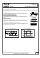
9. A
CTIVE
S
IGNAL
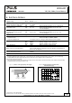
The signal “Active” (pin 7) is an opto-coupler output which is low ohmic while buffer capacitors are discharged.
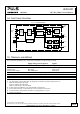
Wiring scheme see Fig. 8-2, Fig. 25-1 and Fig. 25-2.
Signal voltage
Max. 35Vdc Voltage between pin 6 and 7
Signal current
Max. 10mA
Voltage drop across opto
-coupler 0.9V / 3V At 1mA / 5mA while opto-coupler is low ohmic
Leakage current
Max. 50µA While opto-coupler is high ohmic
Isolation voltage
See chapter 21.
10. R
EADY
S
IGNAL
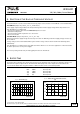
The signal “Ready” (pin 8) is an opto-coupler output which is low ohmic when buffer capacitors are fully charged.
Wiring scheme see Fig. 8-2, Fig. 25-1 and Fig. 25-2.
Signal voltage
Max. 35Vdc Voltage between pin 6 and 8
Signal current
Max. 10mA
Voltage drop across opto
-coupler 0.9V / 3V At 1mA / 5mA while opto-coupler is low ohmic
Leakag
e current Max. 50µA While opto-coupler is high ohmic
Isolation voltage
See chapter 21.
11. I
NHIBIT
I
NPUT
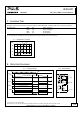
Buffering can be disabled or interrupted with the inhibit input (pin 9). Therefore, pin 6 should be connected to the
positive pole of the terminal voltage or to the external control voltage and pin 9 must be connected to the
corresponding negative pole.
Inhibiting the unit also discharges the internal capacitors. Charging of the capacitor is not possible when the buffer
module is in inhibit mode.
Wiring scheme see Fig. 8-2, Fig. 25-1 and Fig. 25-2.
Signal voltage
Max. 35Vdc (between pin 6 and pin 9)
Signal current
Max.
4mA, current limited
Inhibit mode
The unit does not buffer (or stops buffering) if the voltage between pin 6 and pin 9 is
higher than 10V. Below 6V buffering will function again.
Isolation voltage
See chapter 21.