
Owner manual


Chapter 2 Specifications
2-5
2.2.2 Output Specifications
RISK OF UNINTENDED EQUIPMENT OPERATION
Failure to follow this instruction can result in death, serious injury or equipment damage.
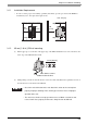
Source Transistor Output Characteristics Q0,Q1
Do not exceed the recommended temperature / simultaneous I/O usage guidelines.
Exceeding the temperature and / or simultaneous I/O in the “on” state can cause
overheating of HTB and / or the I/O expansion modules, resulting in unexpected operation
of the inputs and outputs. Depending on the I/O configuration, unintended equipment
operation can occur.
Output type Source output
Output points per common Line 2
Rated load voltage DC24 V
Maximum load current 1 A per common line
Operating load voltage range from DC20.4 to 28.8 V
Voltage drop (on voltage)
DC1 V (max.) (voltage between COM and
output terminals when output is on)
Rated load current 0.3 A per output
Inrush current 1 A (max.)
Leakage current 0.1 mA (max.)
Clamping voltage DC39 V ±1 V
Maximum lamp load 8 W
Inductive load L/R = 10 ms (DC28.8 V, 1 Hz)
External current draw
100 mA (max.), DC24 V
(power voltage at the -V terminal)
Isolation
Between output terminal and internal circuit:
photocoupler isolated (isolation protection up
to AC500 V rms)
Between output terminals: not isolated
Average number of connector insertions/
removals
100 times (min.)
Output delay - turn on time 5 µs (max.)
Output delay - turn off time 5 µs (max.)