
Specifications


Zylogic ZE5 Configurable System-on-Chip Platform
www.Zylogic.com.cn 116
P
P
r
r
o
o
g
g
r
r
a
a
m
m
m
m
a
a
b
b
l
l
e
e
I
I
n
n
p
p
u
u
t
t
/
/
O
O
u
u
t
t
p
p
u
u
t
t
(
(
P
P
I
I
O
O
)
)
T
T
i
i
m
m
i
i
n
n
g
g
G
G
u
u
i
i
d
d
e
e
l
l
i
i
n
n
e
e
s
s
Q
EN
D
Flip-Flop/
Latch
Input
Registered
Input
Clock
Clock
Enable
Input
Hysteresis
PAD
BusMinder™
Output
Enable
Drive
Strength
Output
Delay
Zero Hold
Time
D
EN
Q
D
EN
Q
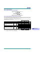
Figure 81. Programmable Input/Output (PIO).
I
I
n
n
p
p
u
u
t
t
P
P
a
a
t
t
h
h
C
C
h
h
a
a
r
r
a
a
c
c
t
t
e
e
r
r
i
i
s
s
t
t
i
i
c
c
s
s
The values listed below are representative, guideline values extracted from measured internal test pat-
terns. Actual values may depend on application-specific use. FastChip reports specific, worst-case guar-
anteed values in the Timing Analysis section of the project report.
All timing parameters assume worst-case operating conditions, including process technology, power sup-
ply voltage, and junction temperature. Values include delay driving one interconnect segment.
Guideline Guideline
Speed Grade -25 -40
Description Symbol Fig. Device Min Max Min Max Units
Propagation Delays
Pad to input [1] T
PID
36 All 4.2 2.5 ns
Pad to registered input via trans-
parent input latch, no delay [1]
T
PIL
36 All 4.5 3.5 ns
PIO clock input on to registered
input IQ, flip-flop mode [1]
T
PICQ
36 All 4.5 2.9 ns
PIO clock input on to registered
input IQ, transparent latch mode [1]
T
PICL
36 All 4.4 2.9 ns
Setup Time before PIO clock CK
Clock enable T
PENS
36 All 2.0 1.5 ns
Pad, zero hold time delay inserted T
PPS
36 All 2.0 1.5 ns
Pad, no delay inserted T
PPSN
36 All 0 0 ns
Hold Time after PIO clock CK
Pad or clock enable, zero hold time
delay inserted
T
PENH
36 All 0 0 ns
Pad or clock enable, no delay in-
serted
T
PNHN
36 All 3.1 2.3 ns
PIO Clock
Clock High time T
PCH
36 All 2.5 1.8 ns
Clock Low time T
PCL
36 All 7.8 5.7 ns
Guideline Guideline
Note 1:
Includes output delay driving onto a single interconnect segment, T
ZIP