
Specifications


115 www.zylogic.com.cn
B
B
u
u
s
s
C
C
l
l
o
o
c
c
k
k
a
a
n
n
d
d
G
G
l
l
o
o
b
b
a
a
l
l
B
B
u
u
f
f
f
f
e
e
r
r
s
s
B
B
u
u
s
s
C
C
l
l
o
o
c
c
k
k
a
a
n
n
d
d
G
G
l
l
o
o
b
b
a
a
l
l
B
B
u
u
f
f
f
f
e
e
r
r
s
s
F
F
u
u
n
n
c
c
t
t
i
i
o
o
n
n
a
a
l
l
D
D
i
i
a
a
g
g
r
r
a
a
m
m
PAD
BCLK/XTAL
PAD
GBUFx
BusClock
GBufx
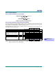
Figure 80. Bus Clock and Global Buffers.
B
B
u
u
s
s
C
C
l
l
o
o
c
c
k
k
a
a
n
n
d
d
G
G
l
l
o
o
b
b
a
a
l
l
B
B
u
u
f
f
f
f
e
e
r
r
s
s
T
T
i
i
m
m
i
i
n
n
g
g
C
C
h
h
a
a
r
r
a
a
c
c
t
t
e
e
r
r
i
i
s
s
t
t
i
i
c
c
G
G
u
u
i
i
d
d
e
e
l
l
i
i
n
n
e
e
s
s
The values listed below are representative, guideline values extracted from measured internal test pat-
terns. Actual values may depend on application-specific use. FastChip reports specific, worst-case guar-
anteed values in the Timing Analysis section of the project report.
All timing parameters assume worst-case operating conditions, including process technology, power sup-
ply voltage, and junction temperature.
Guideline Guideline
Speed Grade -25 -40
Description Symbol Fig. Device Maximum Maximum
Units
Bus Clock
ZE502 5.7 4.3 ns
ZE505 5.7 4.3 ns
ZE512 5.7 4.3 ns
From BCLK/XTAL input through bus
clock buffer to any CSL or PIO clock
input CK [1]
T
BCLK
34
ZE520 5.7 4.3 ns
Global Buffers
ZE502 7.1 5.5 ns
ZE505 7.1 5.5 ns
ZE512 7.1 5.5 ns
From GBUFx input through associated
global buffer to any CSL or PIO input
[2]
T
GBUF
34
ZE520
7.1 5.5 ns
Guideline Guideline
Note 1:
Values for all devices based on data measured on a ZE520. The delays for the ZE502, ZE505, and
ZE512 are expected to be less than the ZE520.
批注 [SKK31]: All –25
numbers are –40 times 1.3