
Specifications


111 www.zylogic.com.cn
C
C
o
o
n
n
f
f
i
i
g
g
u
u
r
r
a
a
b
b
l
l
e
e
S
S
y
y
s
s
t
t
e
e
m
m
L
L
o
o
g
g
i
i
c
c
(
(
C
C
S
S
L
L
)
)
C
C
e
e
l
l
l
l
(
(
M
M
e
e
m
m
o
o
r
r
y
y
M
M
o
o
d
d
e
e
,
,
S
S
i
i
n
n
g
g
l
l
e
e
-
-
P
P
o
o
r
r
t
t
R
R
A
A
M
M
)
)
In memory mode, a single CSL cell implements a 16x1, edge-triggered, single-port random-access mem-
ory (RAM). Two CSL cells in tandem operate as a 32x1, edge-triggered RAM. The outputs can be cap-
tured in the CSL cell's flip-flop.
C
C
S
S
L
L
M
M
e
e
m
m
o
o
r
r
y
y
M
M
o
o
d
d
e
e
,
,
S
S
i
i
n
n
g
g
l
l
e
e
-
-
P
P
o
o
r
r
t
t
R
R
A
A
M
M
F
F
u
u
n
n
c
c
t
t
i
i
o
o
n
n
a
a
l
l
D
D
i
i
a
a
g
g
r
r
a
a
m
m
s
s
16x1 RAM
A3
A2
A1
A0
DI
WE
CK
O
Figure 74. 16x1 single-port RAM.
32x1 RAM
A4
A3
A2
DI
WE
CK
O
A1
A0
Figure 75. 32x1 single-port RAM.
C
C
S
S
L
L
M
M
e
e
m
m
o
o
r
r
y
y
M
M
o
o
d
d
e
e
,
,
S
S
i
i
n
n
g
g
l
l
e
e
-
-
P
P
o
o
r
r
t
t
R
R
A
A
M
M
T
T
i
i
m
m
i
i
n
n
g
g
C
C
h
h
a
a
r
r
a
a
c
c
t
t
e
e
r
r
i
i
s
s
t
t
i
i
c
c
G
G
u
u
i
i
d
d
e
e
l
l
i
i
n
n
e
e
s
s
The values listed below are representative, guideline values extracted from measured internal test pat-
terns. Actual values may depend on application-specific use. FastChip reports specific, worst-case guar-
anteed values in the Timing Analysis section of the project report.
All timing values shown assume worst-case operating conditions, including process technology, power
supply voltage, and junction temperature. Values include delay driving one interconnect segment.
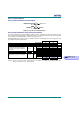
Guideline Guideline
Speed Grade -25 -40
Description Symbol Fig. Size Min Max Min Max
Units
Write Operation
Address write cycle time (clock pe-
riod)
T
WC16
T
WC32
28,30
29,30
16x1
32x1
5.6
5.6
4.1
4.1
ns
CK clock pulse width (active edge)
T
WP16
T
WP32
28,30
29,30
16x1
32x1
3.5
3.5
2.7
2.7
ns
Address setup time before CK
T
AS16
T
AS32
28,30
29,30
16x1
32x1
0.8
0.8
0.6
0.6
ns
Address hold time after CK
T
AH16
T
AH32
28,30
29,30
16x1
32x1
0
0
0
0
ns
DIN setup time before CK
T
DS16
T
DS32
28,30
29,30
16x1
32x1
0.9
0.9
0.7
0.7
ns
DIN hold time after CK
T
DH16
T
DH32
28,30
29,30
16x1
32x1
0
0
0
0
ns
WE setup time before CK
T
WS16
T
WS32
28,30
29,30
16x1
32x1
1.6
1.6
1.2
1.2
ns
WE hold time after CK
T
WH16
T
WH32
28,30
29,30
16x1
32x1
0
0
0
0
ns
Data valid at O after CK [1]
T
WO16
T
WO32
28,30
29,30
16x1
32x1
7.0
8.0
5.2
6.3
ns
Read Operation
Address read cycle time
T
RC16
T
RC32
28,30
29,30
16x1
32x1
10.5
11.5
7.5
8.4
ns
Data valid after address change (no
Write Enable) [1]
T
AO16
T
AO32
28,30
29,30
16x1
32x1
4.5
5.5
3.0
4.0
ns
Guideline Guideline
Note 1:
Includes output delay driving onto a single interconnect segment, T
ZIP
批注 [SKK20]: Actual data
shows 0.4 ns hold time. To
compensate for positive
hold time, this value shows
the total active window
(Hold-Setup).
批注 [SKK21]: DIN setup
time = 0.1, DIN hold time =
+0.6, total window = 0.7 ns.
–25 is 1.3 x (0.7)
批注 [SKK22]: Hold time
actually measured as –0.5
ns.