
Specifications


Zylogic ZE5 Configurable System-on-Chip Platform
www.Zylogic.com.cn 110
C
C
o
o
n
n
f
f
i
i
g
g
u
u
r
r
a
a
b
b
l
l
e
e
S
S
y
y
s
s
t
t
e
e
m
m
L
L
o
o
g
g
i
i
c
c
(
(
C
C
S
S
L
L
)
)
C
C
e
e
l
l
l
l
(
(
A
A
r
r
i
i
t
t
h
h
m
m
e
e
t
t
i
i
c
c
M
M
o
o
d
d
e
e
)
)
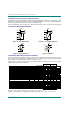
In arithmetic mode, a CSL implements a single bit preloadable adder or subtracter. Alternatively, a CSL
implements a single-bit adder/subtracter with a separate add/subtract control. As a single-bit multiplier, a
CSL cell has a partial-sum input from the previous multiplier stage.
As with combinatorial logic, the outputs from an arithmetic function can be stored in the CSL cell's flip-flop.
C
C
S
S
L
L
A
A
r
r
i
i
t
t
h
h
m
m
e
e
t
t
i
i
c
c
M
M
o
o
d
d
e
e
F
F
u
u
n
n
c
c
t
t
i
i
o
o
n
n
a
a
l
l
D
D
i
i
a
a
g
g
r
r
a
a
m
m
s
s
1
0
+
+
X
Y
LD
DI
CI
CO
Figure 70. Preloadable Adder.
1
0
-
+
CO
CI
LD
Y
X
DI
Figure 71. Preloadable Subtracter.
±
+
CO
CI
SUB
Y
X
Figure 72. Adder/Subtracter.
CO
CI
X
Y
PS
Figure 73. Multiplier.
C
C
S
S
L
L
A
A
r
r
i
i
t
t
h
h
m
m
e
e
t
t
i
i
c
c
M
M
o
o
d
d
e
e
T
T
i
i
m
m
i
i
n
n
g
g
C
C
h
h
a
a
r
r
a
a
c
c
t
t
e
e
r
r
i
i
s
s
t
t
i
i
c
c
G
G
u
u
i
i
d
d
e
e
l
l
i
i
n
n
e
e
s
s
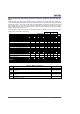
The values listed below are representative, guideline values extracted from measured internal test pat-
terns. Actual values may depend on application-specific use. FastChip reports specific, worst-case guar-
anteed values in the Timing Analysis section of the project report.
All timing values shown assume worst-case operating conditions, including process technology, power
supply voltage, and junction temperature.
Guideline Guideline
Speed Grade -25 -40
Description Symbol Fig. Device Min Max Min Max Units
All Arithmetic Functions
Operands X, Y to SUM output [1] T
OPS
24-27 All 4.5 3.1 ns
CI input to SUM output [1] T
CIS
24-27 All 4.9 3.3 ns
Operands X, Y to CO output [1,2] T
OPC
24-27 All 5.5 3.8 ns
CI input to CO output [1,2] T
CCOA
24-27 All 4.2 1.6 ns
Adder or Subtracter Only
DI data input to SUM output [1] T
DIS
24,25 All 3.9 2.6 ns
DI data input to CO output [1,2] T
DICO
24,25 All 6.3 3.6 ns
LD load input to SUM output [1] T
LDS
24,25 All 3.3 2.3 ns
LD load input to CO output [1,2] T
LDCO
24,25 All 6.3 3.4 ns
Adder/Subtracter Only
SUB add/subtract input to SUM output [1] T
SUS
26 All 3.3 2.3 ns
SUB add/subtract input to CO output [1,2] T
SCO
26 All 5.6 3.4 ns
Multiplier Only
PS partial sum input to SUM output [1] T
PS
27 All 4.5 3.0 ns
PS partial sum input to CO output [1,2] T
PCO
27 All 5.5 3.3 ns
Guideline Guideline
Note 1:
Includes output delay driving onto a single interconnect segment, T
ZIP
Note 2:
If CO output drives CI of adjacent block, subtract output delay, T
ZIP
, 1.4 ns for -25, 0.7 ns for -40