
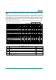
Specifications


109 www.zylogic.com.cn
C
C
S
S
L
L
C
C
o
o
m
m
b
b
i
i
n
n
a
a
t
t
o
o
r
r
i
i
a
a
l
l
L
L
o
o
g
g
i
i
c
c
a
a
n
n
d
d
S
S
e
e
q
q
u
u
e
e
n
n
t
t
i
i
a
a
l
l
M
M
o
o
d
d
e
e
T
T
i
i
m
m
i
i
n
n
g
g
C
C
h
h
a
a
r
r
a
a
c
c
t
t
e
e
r
r
i
i
s
s
t
t
i
i
c
c
G
G
u
u
i
i
d
d
e
e
l
l
i
i
n
n
e
e
s
s
The values listed below are representative, guideline values extracted from measured internal test pat-
terns. Actual values may depend on application-specific use. FastChip reports specific, worst-case guar-
anteed values in the Timing Analysis section of the project report.
All timing values shown assume worst-case operating conditions, including process technology, power
supply voltage, and junction temperature.
Guideline Guideline
Speed Grade -25 -40
Description Symbol Fig. Device Min Max Min Max
Units
Combinatorial Functions
Four-input logic function or 16x1 ROM,
inputs I3 - I0 to O output, no output driver
delay [1]
T
ILO
20 All 3.1 2.4 ns
Four-input logic function or 16x1 ROM,
inputs I3 - I0 to O output [2]
T
LUT4
20 All 4.5 3.1 ns
Five-input logic function or 32x1 ROM,
inputs I4 - I0 to O output [2]
T
LUT5
21 All 5.5 4.0 ns
Six- to nine-input logic function, inputs I8 -
I0 to O output [2]
T
LOG9
22 All 5.5 4.0 ns
Cascaded, Wide Functions
Cascaded four-input logic function or 16x1
ROM, inputs I3 - I0 to CO output [2, 3]
T
LCO4
20 All 6.9 4.0 ns
Cascaded logic function WIDE4, input CI
to CO output [2, 3]
T
CCO4
20 All 4.3 2.9 ns
Cascaded five-input logic function or 32x1
ROM, inputs I4 - I0 to CO output [2, 3]
T
LCO5
21 All 5.5 4.0 ns
Cascaded logic function WIDE5, input CI
to CO output [2, 3]
T
CCO5
21 All 4.1 3.4 ns
Sequential Delays
CSL cell clock input CK to flip-flop output
Q [2]
T
CKO
14 All 4.0 2.9 ns
Setup Time before CSL Cell Clock CK
LUT4 or 16x1 ROM inputs I3 - I0 to flip-
flop D input
T
LIK4
20 All 5.1 4.0 ns
LUT5 or 32x1 ROM inputs I4 - I0 to flip-
flop D input
T
LIK5
21 All 6.1 4.8 ns
Logic inputs I8 - I0 to flip-flop D input T
LIK9
22 All 6.1 4.8 ns
Cascade input, CI T
CIIK
All 4.9 3.7 ns
Direct input, DI, bypassing LUT T
DIK
23 All 2.0 1.5 ns
Clock enable input CE T
CEK
23 All 1.1 0.9 ns
Hold Time after CSL Cell Clock
All hold times T
CQH
23 All 0 0 ns
CSL Cell Clock
Clock High time, internally generated T
CHC
23 All 2.5 2.0 ns
Clock Low time, internally generated T
CLC
23 All 2.5 2.2 ns
Asynchronous Control Input
Pulse width (High) T
APW
23 All 0.7 0.5 ns
Delay from Asynchronous input asserted
to Q
T
AQ
23 All 1.9 1.5 ns
CSL Toggle Frequency
Toggle frequency, Q output through local
interconnect, through LUT4, to setup on
flip-flop [4]
F
TGL
20 All 123.7 158.8 MHz
Guideline Guideline
Note 1:
Calculated using methods similar to other programmable logic vendors
Note 2:
Includes output delay driving onto a single interconnect segment, T
ZIP
Note 3:
If CO output drives CI of adjacent block, subtract output delay, T
ZIP
, 1.4 ns for -25, 0.7 ns for -40
Note 4:
Derived from FastChip test design
批注 [SKK18]: Using clock
High time from PIO provided
by Ed
批注 [SKK19]: Using clock
Low time from PIO provided
by Ed