
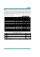
Specifications


105 www.zylogic.com.cn
C
C
S
S
I
I
S
S
o
o
c
c
k
k
e
e
t
t
T
T
i
i
m
m
i
i
n
n
g
g
C
C
h
h
a
a
r
r
a
a
c
c
t
t
e
e
r
r
i
i
s
s
t
t
i
i
c
c
G
G
u
u
i
i
d
d
e
e
l
l
i
i
n
n
e
e
s
s
The values listed below are representative, guideline values extracted from measured internal test pat-
terns. Actual values may depend on application-specific use. FastChip reports specific, worst-case guar-
anteed values in the Timing Analysis section of the project report.
Guideline Guideline
Speed Grade -25 -40
Description Symbol Fig. Device Typical Typical
Units
Bus Write Operations
Data Write valid, distributed and setup before
writing to byte-wide register, through 4-input LUT
T
CDWD
12 All 8.0 16.0 6.0 12.0 ns
Additional logic and interconnect delay allowed
in Data Write path to byte-wide register, through
4-input LUT, operating at maximum clock fre-
quency, F
BCLK
T
BCYC -
T
CDWD
12 All 24.0 32.0 13.0 19.0 ns
Data Write valid, distributed and setup to 16x8
RAM
T
CDWR
13 All 8.0 16.0 6.0 12.0 ns
Additional logic and interconnect delay allowed
in Data Write path to 16x8 RAM, operating at
maximum clock frequency, F
BCLK
T
BCYC -
T
CDWR
13 All 24.0 32.0 13.0 19.0 ns
Selector output valid (WrSel, Sel, or AckSel),
distributed and setup before writing to byte-wide
register
T
CDWS
12 All 12.0 28.0 7.0 15.0 ns
Additional logic and interconnect delay allowed
in Selector path to byte-wide register, operating
at maximum clock frequency, F
BCLK
T
BCYC -
T
CDWS
12 All 12.0 28.0 10.0 18.0 ns
Selector output valid (WrSel, Sel, or AckSel),
distributed and setup before writing to 16x8 RAM
T
CDWE
13 All 12.0 28.0 7.0 15.0 ns
Additional logic and interconnect delay allowed
in Selector path to 16x8 RAM, operating at
maximum clock frequency, F
BCLK
T
BCYC -
T
CDWE
13 All 12.0 28.0 10.0 18.0 ns
Address valid, distributed and setup before writ-
ing to 16x8 RAM
T
CDWA
13 All 15.0 19.0 8.0 12.0 ns
Additional logic and interconnect delay allowed
in Address path to 16x8 RAM, operating at
maximum clock frequency, F
BCLK
T
BCYC -
T
CDWA
13 All 11.0 25.0 13.0 17.0 ns
Bus Read Operations
Data output Q valid on byte-wide register, dis-
tributed and setup before read operation
T
CDRD
14 All 5.0 10.0 5.0 10.0 ns
Additional logic and interconnect delay allowed
in Data Read path from Q output on byte-wide
register, operating at maximum clock frequency,
F
BCLK
T
BCYC -
T
CDRD
14 All 15.0 20.0 15.0 20.0 ns
Data output O valid on 16x8 RAM, distributed
and setup before read operation
T
CDRR
15 All 9.0 19.0 7.0 14.0 ns
Additional logic and interconnect delay allowed
in Data Read path from O output on 16x8 RAM,
operating at maximum clock frequency, F
BCLK
T
BCYC -
T
CDRR
15 All 11.0 21.0 11.0 18.0 ns
Selector output valid (RdSel, Sel, or AckSel),
distributed and setup before read operation
T
CDRS
14,
15
All 12.0 28.0 9.0 14.0 ns
Additional logic and interconnect delay allowed
in Data Read, Selector output to Enable, operat-
ing at maximum clock frequency, F
BCLK
T
BCYC -
T
CDRS
14,
15
All 12.0 28.0 11.0 16.0 ns
Address valid, distributed to 16x8 RAM, data
output O valid, distributed and setup before read
operation
T
CDRC
15 All 20.0 30.0 15.0 17.0 ns
Additional logic and interconnect delay allowed
in Data Read, Address through 16x8 output O,
operating at maximum clock frequency, F
BCLK
T
BCYC -
T
CDRC
15 All 10.0 20.0 8.0 10.0 ns
Guideline Guideline