
Specifications


103 www.zylogic.com.cn
C
C
o
o
n
n
f
f
i
i
g
g
u
u
r
r
a
a
b
b
l
l
e
e
S
S
y
y
s
s
t
t
e
e
m
m
I
I
n
n
t
t
e
e
r
r
c
c
o
o
n
n
n
n
e
e
c
c
t
t
(
(
C
C
S
S
I
I
)
)
S
S
o
o
c
c
k
k
e
e
t
t
T
T
i
i
m
m
i
i
n
n
g
g
G
G
u
u
i
i
d
d
e
e
l
l
i
i
n
n
e
e
s
s
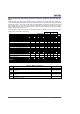
The Zylogic Configurable System Interconnect (CSI) bus socket provides a family-independent interface
between the processor, its peripherals, and the Configurable System Logic (CSL) matrix. The following
values provide a typical range of worst-case delays based on test designs. The actual values depend on
a variety of factors including how the CSL logic cells connect to the CSI bus in the application, the utiliza-
tion of the CSL matrix, and the number of modules in the design. The tables also show how much addi-
tional logic delay, or slack time, is allowed in each type of logic path while operating at the maximum bus
clock frequency,
F
BCLK
.
C
C
S
S
I
I
S
S
o
o
c
c
k
k
e
e
t
t
F
F
u
u
n
n
c
c
t
t
i
i
o
o
n
n
a
a
l
l
D
D
i
i
a
a
g
g
r
r
a
a
m
m
32
Address
Data Write
8
DMA ReqSel
WaitNext
Break
Selector RdSel
Selector WrSel
ChipSel RdSel
ChipSel Sel
DMA AckSel
Waited
Event
Bus Clock
Data
Address
Selector
ChipSel
DMACtrl
WaitCtrl
BrkPnt
BusClk
8
Data Read
Enable
Figure 57. Configurable System Interconnect (CSI) bus socket.
C
C
S
S
I
I
S
S
o
o
c
c
k
k
e
e
t
t
T
T
i
i
m
m
i
i
n
n
g
g
B
B
e
e
n
n
c
c
h
h
m
m
a
a
r
r
k
k
C
C
i
i
r
r
c
c
u
u
i
i
t
t
s
s
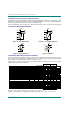
D
EN
Data Write
WrSel, Sel, AckSel
Bus Clock
Q
CSI Bus
Socket
8
Byte-Wide
Data Register
Figure 58. CSI bus write to byte-wide register.
4
DI
WE
Data Write
WrSel, Sel, AckSel
Bus Clock
O
CSI Bus
Socket
8
16x8 RAM
AAddress
Figure 59. CSI bus write to 16x8 RAM.
8
D
ENRdSel, Sel, AckSel
Q
CSI Bus
Socket
Byte-Wide
Data Register
Data Read
Enable
Figure 60. CSI bus read from byte-wide register.
4
8
Data ReadDI
WE
O
16x8 RAM
AAddress
EnableRdSel, Sel, AckSel
CSI Bus
Socket
Figure 61. CSI bus read from 16x8 RAM.