
Specifications


Zylogic ZE5 Configurable System-on-Chip Platform
www.Zylogic.com.cn 102
A
A
s
s
y
y
n
n
c
c
h
h
r
r
o
o
n
n
o
o
u
u
s
s
M
M
e
e
m
m
o
o
r
r
y
y
I
I
n
n
t
t
e
e
r
r
f
f
a
a
c
c
e
e
T
T
i
i
m
m
i
i
n
n
g
g
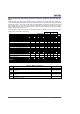
The following values are derived from MIU tests where Bus Clock is provided via an external source.
While using the internal crystal oscillator amplifier or the internal ring oscillator, Bus Clock may not be
externally visible. The following values provide relative timing referencing only signals available on the
MIU. The timing of the MIU control signals is determined by the bit settings in the MIU control register, as
shown in
Table 46.
For supported memory devices, FastChip automatically configures the proper pulse width and strobe set-
tings based on the speed of the selected device and the frequency of Bus Clock.
Preliminary Preliminary
Speed Grade -25 -40
Description Symbol Fig. Device
Start Here
Add Min
or Max
Variable Timing [1] Min Max Min Max Units
Address valid after CE-
asserted
T
MCAD
8,9,10 All N/A 0 2.0 0 2.0 ns
Address hold time after CE-
de-asserted
T
MADC
8,9,10 All N/A 0 3.0 0 1.5 ns
Read Timing
8032 fetch (read) access time
[2]
T
MRAC
8,9 All
[(RSU+RPW+1)• T
BCYC
]
+ Min
-28.0
-20.0 ns
CE- pulse width, read T
MCER
8,9 All
[(RSU+RPW+1)• T
BCYC
]
+ Max
-2.0 -1.5 ns
OE- asserted after CE-
asserted, read [3]
T
MCOE
8,9 All
(RSU• T
BCYC
) + T
BCH
+ Min
-2.0
-1.5 ns
OE- pulse width, read [3] T
MOEP
8,9 All
(RPW• T
BCYC
) + T
BCL
+ Max
-2.0 -1.5 ns
Read data on D[7:0] setup
time before OE- de-asserted
T
MDOE
8,9 All N/A 23.0 17.0 ns
CE- de-asserted after OE-
de-asserted
T
MOEC
8,9 All N/A 2.0 1.5 ns
Data float time after OE-
de-asserted
T
MZOE
8,9 All N/A 0 7.0 0 5.0 ns
Write Timing
CE- pulse width, write T
MCEW
8,10 All
[(WSU+WPW+WHT+1)•
T
BCYC
]+ Max
-2.0 -1.5 ns
WE- asserted after CE-
asserted, write [3]
T
MCWE
8,10 All
(WSU• T
BCYC
) + T
BCH
+ Min
-2.5 -1.5 ns
WE- pulse width, write [3] T
MWEP
8,10 All
(WPW• T
BCYC
) + T
BCL
+ Max
-2.0 -1.5 ns
Write data valid on D[7:0]
after WE-asserted
T
MDWE
8,10 All NA 0 2.0 0 2.0 ns
Write data hold time after
WE- de-asserted
T
MDHW
8,10 All
(WHT• T
BCYC
)
+ Min or Max
0 +2.5 0 +1.5 ns
CE- de-asserted after WE-
de-asserted
T
MWEC
8,10 All
(WHT• T
BCYC
)
+ Max or Max
0 +2.0 0 +2.0 ns
Preliminary Preliminary
Note 1:
The MIU control register controls the timing for the read setup time (RSU), the read pulse width (RPW),
the write setup time (WSU), the write pulse width (WPW), and the write hold time (WHT).
Table 46
shows the legal values for each parameter. The MIU control register timings do not affect ex-
ternal accesses controlled by Selectors in the CSL matrix.
Note 2:
The 8032 microcontroller operates at maximum performance—i.e., no wait-states—when RSU=0 and
RPW=2, resulting in a 3 clock-cycle read strobe.
Note 3:
If the source for Bus Clock is an external clock driver with known characteristics, use the actual minimum
clock High and clock Low times for the clock source. In all other cases, assume the minimum times, T
BCH
and T
BCH
.
批注 [SKK5]: (TMAA-
TMCED)
批注 [SKK6]: (RSU+RPW+
1)•TBCYC - (TMCEA-
TMCED)
批注 [SKK7]: RSU•TBCYC
+TBCH - (TMCEA-TMOEA)
批注 [SKK8]: RPW•TBCYC
+ TBCL-(TMOEA-TMOED)
批注 [SKK9]: TMDSU+TM
OED
批注 [SKK10]: | TMOED-
MCED |
批注 [SKK11]: | TMDRZ-
TMOED |
批注 [SKK12]: (WSU+WPW
+WHT+1)•TBCYC -
(TMCEA-TMCED)
批注 [SKK13]: WSU•TBCY
C +TBCH - (TMCEA-
TMWEA)
批注 [SKK14]: WPW•TBCY
C + TBCL - (TMWEA-
TMWED)
批注 [SKK15]: | TMDWA-
TMWEA |
批注 [SKK16]: WHT•TBCY
C - (TMWED-TMDWA)
批注 [SKK17]: WHT•TBCY
C - (TMWED-TMCED)