
Specifications


101 www.zylogic.com.cn
M
M
e
e
m
m
o
o
r
r
y
y
I
I
n
n
t
t
e
e
r
r
f
f
a
a
c
c
e
e
U
U
n
n
i
i
t
t
(
(
M
M
I
I
U
U
)
)
T
T
i
i
m
m
i
i
n
n
g
g
C
C
h
h
a
a
r
r
a
a
c
c
t
t
e
e
r
r
i
i
s
s
t
t
i
i
c
c
G
G
u
u
i
i
d
d
e
e
l
l
i
i
n
n
e
e
s
s
,
,
S
S
t
t
a
a
n
n
d
d
-
-
a
a
l
l
o
o
n
n
e
e
O
O
p
p
e
e
r
r
a
a
t
t
i
i
o
o
n
n
(
(
S
S
L
L
A
A
V
V
E
E
-
-
=
=
H
H
i
i
g
g
h
h
)
)
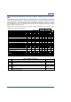
All Zylogic devices are 100% functionally tested. These parameters are modeled after the testing meth-
ods described by MIL-M-38510/605. Pin-to-pin timing parameters are derived by measuring external and
internal test patterns. The values listed below are representative for typical pin locations and normal
clock loading. For these tests, Bus Clock is supplied externally via the BCLK pin. Actual values may de-
pend on application-specific use. FastChip reports specific, worst-case guaranteed values in the Timing
Analysis section of the project report.
All timing values shown assume worst-case operating conditions, including process technology, power
supply voltage, and junction temperature.
Preliminary Preliminary
Speed Grade
-25 -40
Description Symbol Fig. Device Min Max Min Max Units
Bus Clock
Bus Clock frequency F
BCLK
8,9,10 All 0 25.0 0 40.0 MHz
Bus Clock cycle period T
BCYC
8,9,10 All 40.0
∞
25.0
∞
ns
Bus Clock High time T
BCH
8,9,10 All 12.0 12.0 ns
Bus Clock Low Time T
BCL
8,9,10 All 12.0 12.0 ns
Enables
Bus Clock rising edge to CE- asserted T
MCEA
8,9,10 All 24.0 18.0 ns
Bus Clock rising edge to CE- de-asserted T
MCED
8,9,10 All 22.0 16.5 ns
Bus Clock falling edge to OE- asserted T
MOEA
8,9 All 22.0 16.5 ns
Bus Clock to rising edge OE- de-asserted T
MOED
8,9 All 20.0 15.0 ns
Bus Clock falling edge to WE- asserted T
MWEA
8,10 All 22.0 16.0 ns
Bus Clock rising edge to WE- de-asserted T
MWED
8,10 All 20.0 14.5 ns
Data during Read Operation
Setup time on Data before Bus Clock, read
operation
T
MDSU
8,9 All 3.0 2.0 ns
Data float time (high impedance) after read,
relative to Bus Clock
T
MDRZ
8,9 All 13.0 10.0 ns
Data during Write Operation
Data valid after Bus Clock, write operation T
MDWA
8,10 All 22.5 16.0 ns
Address
Address valid after Bus Clock T
MAA
8,9,10 All 25.0 18.0 ns
Table 46. MIU Control Values.
Value Description Legal Values
RSU Read Setup. Controlled by bits MIUCTRL1[3:1] in the MIU control register.
0, 1, 2, 3, 4, 5, 6, 7
RPW
Read Pulse Width. Controlled by bits
MIUCTRL1[6:4] in the MIU control
register.
0, 1, 2, 3, 4, 5, 6, 7
WSU Write Setup. Controlled by bits MIUCTRL0[2:0] in the MIU control register.
0, 1, 2, 3, 4, 5, 6, 7
WPW
Write Pulse Width. Controlled by bits
MIUCTRL0[5:3] in the MIU control
register.
0, 1, 2, 3, 4, 5, 6, 7
WHT
Write Hold Time. Controlled by bits
MIUCTRL1[0] and MIUCTRL0[7:6] in
the MIU control register.
0, 1, 2, 3, 4, 5, 6, 7