
User's Manual
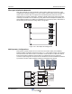


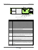
Table Of Contents
- Revision Record
- Table of Contents
- List of Figures
- List of Tables
- Abbreviations
- Chapter 1 Product Description
- Introduction
- Scope of Manual
- Safety
- Warning Signs
- Human Exposure of RF Radiation
- Radiation Safety Distances
- Electrostatic Discharge (ESD)
- Sub Unit Overview
- Wideband Amplifier PCBA (WBA)
- Power Amplifier PCBA (PA)
- Multi-Carrier Power Amplifier PCBA (MCPA)
- Booster Amplifier PCBA (BA)
- Distribution PCBA (DIA)
- Control Unit PCBA (CU)
- Low Noise Amplifier (LNA)
- Duplex Filter (DPX)
- Fiber Optic Unit (FOU)
- Fiber Optic Node (FON)
- Power Supply Unit (PSU)
- Remote Control Unit (RCU)
- Alarm Interface PCBA (ALI) and Remote Control Interface PCBA (RCI)
- Sub Unit Locations
- Fiber Optic Distribution Networks
- Multi-Operator Configurations
- Chapter 2 Controls, Indicators and Connectors
- Chapter 3 Installation
- Chapter 4 Maintenance
- Chapter 5 Specifications
- Appendix A Block Diagrams
Wideband Radio Head PCBA Connectors
2-6 044-05251 Rev A
DPX
DPXs are located on the metal cover sheet in the upper part of the cabinet. Service and
donor filters are identical.
Table 2-7 DPX Connections
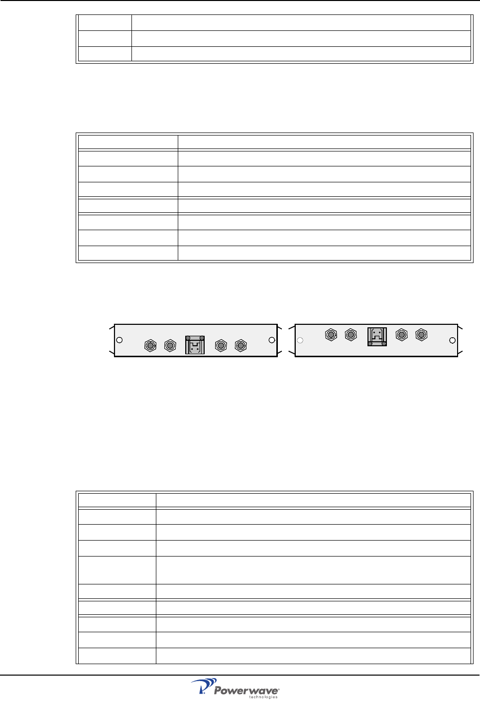
LNA
LNAs are located at the top of the cabinet and the high cover, if equipped. LNA/UL is located
to the left and LNA/DL to the right. All coaxial connectors are SMA-type.
Figure 2-6 Low Noise Amplifiers
Signals from the DPX output are fed to the LNA input connector IN. OUT1 and OUT2 outputs
feed the CHE, CSA, BSA, or WBAs of the same signal direction. The signal level in these
connectors are +20dB referenced to the antenna input. Another output, OUT LOW, is an
expansion output for an additional LNA if the WRH is equipped in the cover part of the
chassis. The gain to this connector is +2dB. The +7V input is used for +7V supply from the
DIA PCBA and ATT is a control signal for a controllable attenuator in the LNA.
Table 2-8 LNA Connections
P34 WLI for IP or R2R network
P35 PSU, connector 2
P36 WLI for IP or R2R network
Service DPX Port Connected to
ANT Service antenna (or DPX on the service (MS) DC
HI P5 on the PA/DL
LO IN on the LNA/UL. P2101 on the WBA PCBA
Donor DPX Port Connected to
ANT ANT on the FOU/DPX filter.
HI IN on the LNA/DL
LO P5 on the PA/UL
LNA/UL Port Connected to
OUT LOW IN on the LNA/UL in the cover, if equipped
IN LO on the service DPX duplex filter.
ATT +7V P23 on the DIA PCBA.
OUT1 P101 on the CHE3/UL, CSA/UL, or BSA/UL PCBA. P2101 on the
WBA PCBA.
OUT2 P101 on the CHE4/UL channel PCBA.
LNA/DL Port Connected to
OUT LOW IN on the LNA/DL in the cover, if equipped
IN HI on the donor DPX duplex filter.
ATT +7V P24 on the DIA PCBA.
OUT
LOW
IN+7V ATTOUT1 OUT2
LNA
DL
OUT
LOW
IN ATT +7V OUT2 OUT1
LNA
UL