
User's Manual

Typical Block Diagram
DCM000000104 Rev Q
1-3
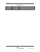
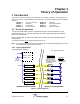
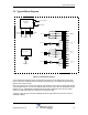
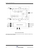
1.3 Typical Block Diagram
Figure 2 Typical Block Diagram
In the LNKFIB-H03 Headend module, the eight fiber optic pairs are in two banks (A & B) of four, with
the RF connections combined inside the module in those groupings. The LNKFIB-H04 is identical, but
with one bank of four removed.
Each of the groups of four consists of a single RF Input feeding a single Laser Transmitter split optically
to four fiber optic outputs. The four matching fiber optic Inputs each go to their own photodiode receiver,
followed by a 0 to -15dB digitally controlled attenuator providing uplink gain control. The RF signals
from the four digital attenuators are combined into a single RF output.
The group of four RF input and output combining inside the module alleviates the need for external
combining / splitting.
SM F.O. In
SM F.O. Out
(PI N Diodes)
(Lasers)
Power Supply
120 / 240 VAC
120/240 VAC
Pre A mp
Laser Diode
Photodetectors & PreAmps
RF O u t " A "
RF Input "A"
SM F.O. In
SM F.O. Out
(PI N Diodes)
(Lasers)
Pre A mp
Laser Diode
Photodetectors & PreAmps
RF O u t " A "
RF Input "A"
With UpLink Gain Control
With UpLink G ain Control
Micro-Controller
Circuitry
CAN Interface RS232 Interface
To Head-End To PC
Green Power On LED
Red Fault LE D
Fault Relay