Reference Manual 1. Abbreviations and Acronyms Abbreviation / Acronym Definition { = Two definitions, { same abbreviation/acronym ACLR....................................................... Adjacent Channel Leakage Power Ratio ACP......................................................... Adjacent Channel Power A/D .......................................................... Analog-to-Digital Conversion ADC.........................................................
ESD......................................................... ElectroStatic Discharge ESG......................................................... Electronic Signal Generator ETDMA.................................................... Extended Time Division Multiple Access ETSI ........................................................ European Telecommunications Standard Institute EUT ......................................................... Equipment Under Test FAR .............................................
M&TE ...................................................... Measuring and Test Equipment NAMPS ................................................... Narrow Analog Mobile Phone System NIOSH..................................................... National Institute for Occupational Safety and Health NIST ........................................................ National Institute for Standards and Technology NMT ........................................................ Nordic Mobile Telephone NVM ...................
SCHPA.................................................... Single-Channel High Power Amplifier SCPA ...................................................... Single Channel Power Amplifier SIM.......................................................... System Interface Module SMA ........................................................ SubMiniature Type A (coaxial connector) SMT......................................................... Surface Mount Technology SN ...................................................
2. Revision History Release Date Jan 23, 2004 May 14, 2004 Revision Level Rev. A Rev. A.01 Rev. B Comments Initial Draft Revised layout (no formatting) Separated sections to independent manuals Significant updates to all text and graphics Correct battery part number in section 4.0 Updated cabinet figures in section 4.0 Minor update to SIM interface in AC Power Wiring Diagrams in section 4.1 Inserted all new documentation for sections 4.7.2 to end of document 3. Introduction 3.
Major System Components Model OPAF-1923-P07C01 Manual 044-05156 044-05162 044-05163 044-05164 044-05122 044-05121 Description Reference Manual Maintenance & Troubleshooting Manual Site Preparation & Installation Manual Field Replaceable Units Manual MCPA Subrack System Interface Module Fan Interface Module 148-Amp Rectifier Low Voltage Disconnect Back-Up Battery Fuse, 600A, 170 VDC or less G3S-1900-125 MCR21929-1-2 800-08824-001 800-09088-001 930-00018-005 * 920-00360-002 * 920-00337-003 TPL-CZ ** * Manu
when the battery voltage drops below 21 VDC. The LVD also provides the trickle charge path for the batteries during recovery and normal operation. The System Interface Module (SIM) monitors the performance and alarm state of the rectifiers, amplifier subracks, and Duplexer Low Noise Amplifier (DLNA) modules.
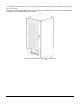
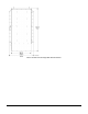
OPAF Front View with Dimensions OPAF Bottom View with Dimensions 044-05156 Rev C 8
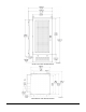
OPAF Left Side View and Right Side with Dimensions 044-05156 Rev C 9
OPAF Front View with Door Removed 044-05156 Rev C 10
OPAF Rear View with Door Removed 044-05156 Rev C 11
MCR21929-1-2 Subrack Front and Rear Isometric View Host Address and Configuration Switches (Covered) APC LED Indicator RS232 Port MCR21929-1-2 Front View without Amplifiers 044-05156 Rev C 12 Gain Adjust
MCR21929-1-2 Subrack Interface Connectors Release Latch G3S-1900-125 Multi-Carrier Power Amplifier Isometric View 044-05156 Rev C 13
G3S-1900-125 Multi-Carrier Power Amplifier- Front, Side and Rear Views DLNA Dimetric View 044-05156 Rev C 14
DLNA Front Panel DLNA Side View Panel System Interface Module 044-05156 Rev C 15
Rear Front 148-Amp Rectifier Isometric Views Rear Front 148-Amp Rectifier Tray and Panel Views 044-05156 Rev C 16
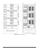
Low Voltage Disconnect (LVD) Module P/N 920-00337-003 Back-Up Battery 4.1 Cabinet Overview This section contains a functional description of the Powerwave OPAF Outdoor Multi-Carrier Power Amplifier (MCPA) System. Refer to the system block diagrams below.
46 Light 2 N/O Rear 48 S2 N/C 50 COM 50 44 GRN 45 49 Light 1 47 N/C 49 COM 43 1 BLU 2 RED 3 WHT 4 YEL Fan Module 1 BLU 2 RED 3 WHT 4 YEL F1 1 BLU 2 RED 3 WHT 4 YEL 1 BLU 2 RED 3 WHT 4 YEL N/O N/O AC 35 N/C Door COM 36 N/O Batt 37 Door N/C COM 38 Front S1 To SIM 34 47, 48 45, H N WHT Load 46 GFCI Outlet Line 44 G 43 20 6 H N 4 5 WHT F2 F3 F4 WHT GRN 6 3 5 2 Ground Bus 8 7 4 B 9 8 Neutral Bus A 7 30 A CB 5 Rectifier 3 30 A CB 4 Rectifier 2 30 A CB 3 Rectifier 1 20 A CB 6 Surge Pr
Controller +53.4dBm 6 6 F WD TX A N T +49dBm R X +12VDC -0.1dB 9 9 E 9 B D 9 I2C F 9 9 9 I2Cm Antenna Power Levels: TX: +52.0dBm (160W) 8 Carriers @ +43.0dBm/Carrier RX: -23.0dBm Max/Carrier -14.0dBmComposite System Interface Module L/A -0.1dB Detector Circuit I 2C C A TX/RXm -0.8dB -0.3dB -3.0dB A +52.1dBm +53.3dBm DLNA0 LNAd -0.2dB 50Ω I2C d FORM-C I2C +27VDC GND 3 1 Detector Circuit RVS 6 +27VDC GND +12VDC +27VDC GND Form-C +21.7dBm Max/Carrier +30.
4.5 G3S-1900-125 Amplifier Module 4.5.1 Overview The G3S-1900-125 amplifier is a linear, feed-forward power amplifier that operates in the 60 MHz frequency band from 1930 MHz to 1990 MHz. It is designed to operate in two continuous frequency blocks in the PCS band or an instantaneous bandwidth of 20 MHz. A typical one-sector system is illustrated above. Each amplifier is a selfcontained plug-in module and is functionally independent of the other amplifier module.
Amplifier Module DC Indicators RF Switch Definition Name +27VDC Indicator +15VDC Indicator +5VDC Indicator -5VDC Indicator Function Green LED. When lit, indicates that the +27 Vdc supply is greater than +21 Vdc and less than +31 Vdc. If the +27 Vdc indicator goes out, the DC Fail indicator will illuminate. This indicates that the +27 Vdc voltage dropped below +21 Vdc. Green LED. When lit, indicates that the +15 Vdc supply is greater than +12 Vdc and less than +17 Vdc.
Amplifier Module RF Control and Indicators Definition Amplifier Alarm System Alarm (From Subrack) MCPA Disable signal (pin 4) AutoRecovery Latching LED MCPA Module Yes Red Disable Major High No Red Disable Major High No Red Enable None Low No Red Disable Major High VSWR No Red Enable None Low VSWR Yes Red Disable Major High DC Fail No Red Disable Major High No Red Disable Major High +27V DC input > 30.5 V 30.
4.5.1.2 Main Amplifier The main amplifier employs class AB amplification for maximum efficiency. The error amplifier and feed forward loops are employed to correct signal nonlinearities introduced by the class AB main amplifier. The error amplifier operates in class AB mode. The RF input signals are amplified by a preamp and coupled to an attenuator and phase shifter in the first feed-forward loop. The main signal is phase shifted by 180 degrees and amplified in the premain amplifier.
Although each amplifier module contains its own heat sink, it is cooled with forced air. Four fans are used for forced air cooling and redundancy. The fans, located on the front and rear of the amplifier module, draw air in through the front of the amplifier and exhaust hot air out the back of the module. The fans are field replaceable. 4.5.
Note 1: Service loop grounded allows the MCPA to be enabled or disabled by the front panel switch when not mounted in the shelf. 4.5.5 Pilot Tone Control The multi-amplifier subracks can be used to control the pilot tone frequency of the installed amplifiers. Pilot tone frequency selection is based on the intended operational band of the amplifiers per the following table.
4.6 MCR21929-1-2 Amplifier Subrack 4.6.1 Overview The MCPA system is a linear, feed-forward power amplifier system that operates in the 60 MHz frequency band from 1930 to 1990 MHz with an instantaneous bandwidth of 20 MHz. It consists of an amplifier subrack with up to two 125-watt G3S-1900-125 plug-in amplifiers. The MCR21929-1-2 houses an RF power splitter/combiner and a control module that monitors the functional status of all plug-in amplifiers.
MCR21919-1-2 Configuration Switch 4.6.1.1.3 APC LED The LED indicator located on the top right-hand corner of the subrack serves several functions. Under normal conditions, the indicator is off. Anytime the APC function is engaged, either from an overdrive or voltage derating situation, the indicator blinks. When the overdrive or voltage derating condition is removed and all the gain is recovered, the indicator ceases to blink and remains off.
MCR21929-1-2 Subrack Input/Output Connectors Reference Number 1 2 Name Function DC Power Terminals GROUND Lug 3 RF OUTPUT Connector 4 RF INPUT Connector 5 RF SAMPLE Connector 6 ALARMS Connector 7 RS-485 Connectors 8 PREAMP Connector 9 RS-232 Connector Base station DC power connections. Subrack chassis ground. Type-N female coax connector, RF output to TX filter and antenna. See table A-1 for power output level of one to two amplifier module systems. SMA female coax connector.
4.6.3.1 Standard Gain Overview and Application (Default Configuration) In the standard gain mode, the gain of the system is dependent on the number of amplifiers operating at a given time and the power from the amplifiers is used at or near their maximum limits. When the design of the cell site requires full power from the amplifiers installed in the subrack in order to achieve maximum call capacity, the standard gain mode should be used.
As the voltage returns to nominal levels, the output power will return accordingly. Sufficient hysteresis of at least 0.1 V is included to eliminate 'toggling' at crossover voltage levels. 4.6.5 Amplifier Monitoring The amplifier alarms are displayed on the front panel indicators and output via a 21-pin connector on the rear of the module to the subrack summary board for subsequent remote monitoring via the ALARMS connector.
Cable is 24 AWG, copper wire stripped and tinned at one end. Indicated state is without DC power applied.
4.6.5.2 RS-485 Connectors (J4, J5) RS-485 signals are monitored through the RS-485 9-pin female D-sub connector on the rear of the subrack. DB9 Connector RS-485 and Preamp Connector Definition PIN 1 2 3 4 5 Description RS-485 TX data + RS-485 TX data RS-485 RX data + RS-485 RX data Ground/Shield PIN 6 7 8 9 Description No Connection No Connection No Connection Ground 4.6.5.
operational band of the amplifiers and must be set during commissioning of the base station, and anytime the MCR21929-1-2 subrack is replaced. Setting the pilot tone frequency of the amplifiers requires a laptop interface program. The laptop can be connected to the MCR21929-1-2’s RS-232 port. The MCR21929-1-2 provides the interface to the amplifiers to set their pilot frequency and stores this setting in memory.
DLNA Front Panel 4.7.3 Transmit Path Overview The transmit path receives amplified RF signals from the MCR21929-1-2 amplifier subrack. The amplified signals are filtered and duplexed with the receive signals and presented to the antenna port. The transmit filter provides 105 dB of isolation in the receive band between the transmit and antenna ports. 4.7.4 DLNA Alarms VSWR and LNA alarms for the DLNA are given on the front panel and sent via an alarm bus to the SIM.
A front panel four-position rotary switch is provided to set the VSWR alarm threshold based on the length of cable from DLNA output (typically FSJ4 or LDF4) to the antenna foam jumper (typically 1 5/8 Heliax). The switch position is set with a jeweler’s screwdriver.
The LNA alarm is sensed within the LNA for both low and high current. A single open collector output is read by the micro-controller and passed on the to I2C interface. 4.8 Power Plant The power plant incorporates EMI filtering, AC surge suppression, a series of circuit breakers, load sharing rectifiers, battery backup, DC power monitoring, and a Low Voltage Disconnect transfer switch. GND Reserved DLNA 0 30 A CB Battery Heater DLNA 1 20 A CB Surge Pro.
Rectifier Subrack Pin Assignments PIN 1 2 3 4 5 6 7 8 Description 5 Vbs 5 Vbs rtn Module Detect Pgood On/off I share Mod-Ena 0VP tp PIN 9 10 11 12 13 14 15 Description AC fail V prog V1 sense I monitor Tem OK Rtn Sense No Connection 4.8.2 Batteries Should the AC input power fail for any reason, four 12 Vdc, 105 AH (rated 8-hour capacity) deep discharge Valveregulated Lead-Acid batteries provide 24 Vdc power for the entire cabinet.
Battery Recharge Cycle from Full Discharge (1.75 V/Cell) to 100% Charge Charger Capacity Battery Voltage Ba tte r Constant Current Stage yC ur re nt Absorpation Mode Float Mode Time Recharge Time 4 x 4KW Modules G3S-1900-125 MCPA Load Time to 80% Recharge (Hours) 1 MCPA 52.8 0.38 2 MCPA 105.6 0.36 3 MCPA 158.4 0.35 4 MCPA 211.2 0.38 5 MCPA 264 0.38 6 MCPA 316.8 0.42 The batteries meet: UL, NEBS, and EUROBAT requirements and have a 10 year plus classification compliance.
The controller also monitors the battery compartment temperature. The output bus voltage is adapted with consideration to the temperature changes of the batteries. The compensation slope is user selectable as one of three values: -36mV/°C (-20mV/°F), –60mV/°C (-33.3mV/°F), and between -10°C (14°F) and 60°C (140°F). The factory setting is –36mV (-3mV/°C/cell). If the probe is not connected or fails to open, the output voltage falls back to factory preset and an alarm is generated.
Switch S1 S100 S12 S11 S9 Pos 1 2 3 4 5 6 7 8 1 2 3 4 5 6 7 8 1 2 3 4 5 6 7 8 1 2 3 4 5 6 7 8 1 2 3 4 5 6 7 8 State Off Off Off Off Off On Off Off On Off Off Off Off Off Off Off Off On On Off On On On On Off Off Off Off Off Off Off Off Off Off Off Off On Off Off Off 044-05156 Rev C Note Switch S7 S5 S10 S8 S6 S4 40 Pos 1 2 3 4 5 6 7 8 1 2 3 4 5 6 7 8 1 2 3 4 5 6 1 2 3 4 5 6 1 2 3 4 5 6 1 2 3 4 5 6 State Off Off Off Off Off Off Off Off On On On Off Off Off Off Off Off Off Off Off On On Off
4.8.4 Low Voltage Disconnect (LVD) Low Voltage Disconnect Module The purpose of the LVD is to monitor the DC bus to regulate the rectifier(s) output voltage with regard to the needed operating voltage to the system, and the appropriate charge voltage for the batteries. Should AC power fail, back-up batteries are installed in the system to provide a relatively short operational period, based on the amplifier load at the time of failure.
LVD Internal Component Locations The controller functions of the LVD are described in the Power Plant Monitoring section of this manual. 4.8.5 Lightning Arrestors Two lightning arrestors located in the AC electrical panel provide added protection to the cabinet when the cabinet is properly grounded. The lightning arrestors are equipped with push-button trip-resets. The lightning arrestors characteristics are given in the specifications section of this manual.
4.
System Interface Module Front and Rear Panels All input/output connections of the SIM are detailed below: I/O J1 J2 J3 J4 J5 J6 J7 J8 J9 J10 J11 J12 J13 J14 J15 J16 J17 J18 J19 J20 J21 Description MCPA0 Serial Interface MCPA1 Serial Interface MCPA2 Serial Interface MCPA3 Serial Interface MCPA4 Serial Interface MCPA5 Serial Interface DLNA0 (Main) Interface DLNA1 (Diversity) Interface DLNA2 (Main) Interface DLNA3 (Diversity) Interface DLNA4 (Main) Interface DLNA5 (Diversity) Interface Rectifier Interface DC
subrack. The SIM is internally terminated, as are each of the amplifier subracks, to prevent loading down the RS485 buss. Pin # 1 2 3 4 5 6 7 8 9 Description RS-485 TX data + RS-485 TX data RS-485 RX data + RS-485 RX data No Connection No Connection No Connection No Connection No Connection Descriptions TX and RX are in reference to the MCPA subrack. TX refers to data in to the SIM. RX refers to data out from the SIM. Amplifier alarms are reported to the SIM via the amplifier subrack RS-485 bus.
The open collector circuit has a 10mA limitation. The interface also includes two auxiliary TTL signals. One is an input and the other an output. The auxiliary output signal is a 74HC14 inverter output. The auxiliary signals have no function at this time. RECT6 signal represents the alarm status of the LVD controller.
PWM VS. Temperature PWM (%) 0 15 25 35 45 55 65 75 85 100 Maximum Temperature +41°C or less +42°C +43°C +44°C +45°C +46°C +47°C +48°C +49°C +50°C or greater There are three fan fault frequency thresholds related to speed control. Fan Fault Thresholds PWM (%) 100 - 50 49 - 20 < 20 Fan Fault Threshold 40Hz 15Hz 10Hz Each fan sense input is measured. If the fan frequency(s) is below the threshold (for the operating mode) for a continuous period of 1-minute a fan fault is reported to the DALI interface.
Display the fan control voltage (0-10) Display the fan speed in Hz Pin # 1 2 3 4 5 Description No Connection RS-232 TX RS-232 RX No Connection Ground Pin # 6 7 8 9 Description No Connection No Connection No Connection No Connection 4.9.5 DALI Interfaces (J15 & J16) The two DALI interfaces are accomplished via two DB25 Female connectors. The DALI interface reports all of the cabinet alarms, excluding the DLNA alarms, to the BTS.
4.9.6 I2C Interfaces - DLNA Main (J17) / Diversity (J18) The two DLNA I2C BTS interfaces are accomplished via two DB25 Female connectors. The DLNA I2C interface is passes-through all of the DLNAs status and module detect signals to the BTS. The I2C interfaces are full duplex and differential (6 I/Os).
5. Specifications Note This Powerwave product is designed to operate within the Normal Operating (typical operating) ranges or conditions specified in this document. Operation of this equipment beyond the specified ranges in this document may cause (1) spurious emissions that violate regulatory rules; (2) the equipment to be automatically removed from service when maximum thresholds are exceeded; or (3) the equipment to not perform in accordance with its specifications.
G3S-1900-125 Multicarrier PCS Amplifier Functional Specifications Frequency Range Total Maximum Input Power Total Output Power Intermodulation Distortion and In-Band Spurious: RF Gain at 1930 MHz Gain Flatness: Gain Variation Over Temperature: Output Protection: Input Port Return Loss: Out of Band Spurious: Duty Cycle: 1930-1990 MHz -4 dBm 125 W typical (1 Module) -63 dBc (Min) @ +26 to +28 Vdc @ 125 Watts DC Input Power: Operating Temperature: Storage Temperature: Operating Humidity: Storage Humidity: RF
MCR21929-1-2 Specifications Frequency Range Power Output / Max Input w/125W modules Duty Cycle RF Gain – Standard (±0.50 dB) RF Gain – Constant (±0.50 dB) RF Gain Adjust Gain Variation with Voltage / Freq.
DLNA Specifications Electrical Characteristics Parameter Limit Unit Transmit (TX) Path specific Frequency Range 1930-1990 MHz Insertion Loss 1.2 dB Loss variation over temperature 0.4 dB In-Band Ripple (J1: TX to J2: Antenna Port) 0.
Parameter Electrical Characteristics Limit Unit Inter modulation Distortion (IMD7) RX Band (J3: RX_01) to (J4: RX_02) -110 dBc -10.0 dBm -18 -18 +20 to +30 27+ 0.5 2 1.5:1 dB dB Vdc Vdc A 1930~1990 -55±2.5 2.0 -18 MHz dB dB dB Remarks Measured @ 1870 MHz.
System Interface Module Specifications Operating Voltage Current Operating Temperature Storage Temperature Humidity Interface Signals Output Voltage Dimensions Weight +27 +0.5 VDC nominal; 20 min to 30 VDC max 5 amps typical; 7.
LVD Specifications Electrical Specifications DC bus connection Nominal voltage User adjustable values Factory set Voltage range Bus voltage monitoring Pre alarm user value range Pre alarm Factory set Battery disconnect range Factory set Rated bus current Battery connections Number of connections Battery type (AH) Temperature compensation Temperature range Slope user adjustable values Factory set Battery protection Fuse rating ranges Factory set Battery Disconnect User settable voltage values Factory set Rec
12 VDC 105 AH Battery Model 920-00337-003 Specifications Cells / Volts Terminal Type Capacity @ 77 ºF (25 ºC) Operating Temperature Charging Voltage / Current Temperature Compensation Storage time from a fully charged condition Self discharge rate AC ripple from charging source Overall dimensions Weight 6 Cells / 12 Volts (DC) Threaded Copper Insert, ¼ inch 105 AH (8 hrs) to 1.75 Volts (DC) per cell -40 ºC to +60 ºC (-40 ºF to +140 ºF) 2.27 to 2.