
Datasheet


TOP242-250
46
I
4/03
General Information & Table of Contents
Product Selector Guide 1
Data Sheets 2
Application Notes 3
Design Ideas 4
Design Tools 5
Quality and Reliability 6
Package Information 7
DPA-Switch
DC-DC Seminar 8
LinkSwitch
&
TinySwitch-II
AC-DC Seminar 9
TOPSwitch-GX
AC-DC Seminar 10
Sales Representatives and Distributors 11
Notes:
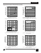
1. Package dimensions conform to JEDEC specification
MS-001-AB (Issue B 7/85) for standard dual-in-line (DIP)
package with .300 inch row spacing.
2. Controlling dimensions are inches. Millimeter sizes are
shown in parentheses.
3. Dimensions shown do not include mold flash or other
protrusions. Mold flash or protrusions shall not exceed
.006 (.15) on any side.
4. Pin locations start with Pin 1, and continue counter-clock-
wise to Pin 8 when viewed from the top. The notch and/or
dimple are aids in locating Pin 1. Pin 6 is omitted.
5. Minimum metal to metal spacing at the package body for
the omitted lead location is .137 inch (3.48 mm).
6. Lead width measured at package body.
7. Lead spacing measured with the leads constrained to be
perpendicular to plane T.
.008 (.20)
.015 (.38)
.300 (7.62) BSC
(NOTE 7)
.300 (7.62)
.390 (9.91)
.367 (9.32)
.387 (9.83)
.240 (6.10)
.260 (6.60)
.125 (3.18)
.145 (3.68)
.057 (1.45)
.068 (1.73)
.120 (3.05)
.140 (3.56)
.015 (.38)
MINIMUM
.048 (1.22)
.053 (1.35)
.100 (2.54) BSC
.014 (.36)
.022 (.56)
-E-
Pin 1
SEATING
PLANE
-D-
-T-
P08B
DIP-8B
PI-2551-041003
D S
.004 (.10)
⊕
T E D S
.010 (.25) M
⊕
(NOTE 6)
SMD-8B
PI-2546-041003
.004 (.10)
.012 (.30)
.036 (0.91)
.044 (1.12)
.004 (.10)
0 -
°
8
°
.367 (9.32)
.387 (9.83)
.048 (1.22)
.009 (.23)
.053 (1.35)
.032 (.81)
.037 (.94)
.125 (3.18)
.145 (3.68)
-D-
Notes:
1. Controlling dimensions are
inches. Millimeter sizes are
shown in parentheses.
2. Dimensions shown do not
include mold flash or other
protrusions. Mold flash or
protrusions shall not exceed
.006 (.15) on any side.
3. Pin locations start with Pin 1,
and continue counter-clock
Pin 8 when viewed from the
top. Pin 6 is omitted.
4. Minimum metal to metal
spacing at the package body
for the omitted lead location
is .137 inch (3.48 mm).
5. Lead width measured at
package body.
6. D and E are referenced
datums on the package
body.
.057 (1.45)
.068 (1.73)
(NOTE 5)
E S
.100 (2.54) (BSC)
.372 (9.45)
.240 (6.10)
.388 (9.86)
.260 (6.60)
.010 (.25)
-E-
Pin 1
D S
.004 (.10)
⊕
⊕
G08B
.420
.046
.060
.060
.046
.080
Pin 1
.086
.186
.286
Solder Pad Dimensions