
Datasheet


TOP242-250
40
I
4/03
General Information & Table of Contents
Product Selector Guide 1
Data Sheets 2
Application Notes 3
Design Ideas 4
Design Tools 5
Quality and Reliability 6
Package Information 7
DPA-Switch
DC-DC Seminar 8
LinkSwitch
&
TinySwitch-II
AC-DC Seminar 9
TOPSwitch-GX
AC-DC Seminar 10
Sales Representatives and Distributors 11
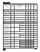
Figure 51. CONTROL Pin I-V Characteristic.
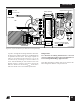
Figure 50. Duty Cycle Measurement.
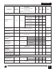
Figure 52. Drain Current Operating Envelope.
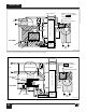
Figure 53. TOPSwitch-GX General Test Circuit.
PI-2631-042303
5-50 V
5-50 V
S4
40 V
0.1 µF47 µF
470 Ω
5 W
Y or R Package (X and L Pin) P or G Package (M Pin)
470 Ω
0-100 kΩ
0-60 kΩ
0-60 kΩ
0-100 kΩ
NOTES: 1. This test circuit is not applicable for current limit or output characteristic measurements.
2. For P and G packages, short all SOURCE pins together.
D
SFX
C
L
M
C
CONTROL
TOPSwitch-GX
S1
S5
S3
0-15 V
S2
PI-2039-033001
DRAIN
VOLTAGE
HV
0 V
90%
10%
90%
t
2
t
1
D =
t
1
t
2
0.8
1.3
1.2
1.1
0.9
0.8
1.0
0
012 6 83
Time (µs)
DRAIN Current (normalized)
PI-2022-033001
45 7
0.7
0.6
0.5
0.4
0.3
0.2
0.1
I
LIMIT(MAX)
@ 25 °C
I
LIMIT(MIN)
@ 25 °C
I
INIT(MIN)
@ 85 VAC
I
INIT(MIN)
@ 265 VAC
t
LEB
(Blanking Time)
120
100
80
40
20
60
0
0246810
CONTROL Pin Voltage (V)
CONTROL Pin Current (mA)
1
Slope
Dynamic
Impedance
=
PI-1939-091996