
Datasheet
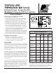


TOP242-250
4
I
4/03
General Information & Table of Contents
Product Selector Guide 1
Data Sheets 2
Application Notes 3
Design Ideas 4
Design Tools 5
Quality and Reliability 6
Package Information 7
DPA-Switch
DC-DC Seminar 8
LinkSwitch
&
TinySwitch-II
AC-DC Seminar 9
TOPSwitch-GX
AC-DC Seminar 10
Sales Representatives and Distributors 11
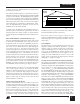
Pin Functional Description
DRAIN (D) Pin:
High voltage power MOSFET drain output. The internal
start-up bias current is drawn from this pin through a switched
high-voltage current source. Internal current limit sense point
for drain current.
CONTROL (C) Pin:
Error amplifier and feedback current input pin for duty cycle
control. Internal shunt regulator connection to provide inter-
nal bias current during normal operation. It is also used as the
connection point for the supply bypass and auto-restart/
compensation capacitor.
LINE-SENSE (L) Pin: (Y, R or F package only)
Input pin for OV, UV, line feed forward with DC
MAX
reduction,
remote ON/OFF and synchronization. A connection to
SOURCE pin disables all functions on this pin.
EXTERNAL CURRENT LIMIT (X) Pin: (Y, R or F
package only)
Input pin for external current limit adjustment, remote
ON/OFF, and synchronization. A connection to SOURCE pin
disables all functions on this pin.
MULTI-FUNCTION (M) Pin: (P or G package only)
This pin combines the functions of the LINE-SENSE (L) and
EXTERNAL CURRENT LIMIT (X) pins of the Y package
into one pin. Input pin for OV, UV, line feed forward with
DC
MAX
reduction, external current limit adjustment, remote
ON/OFF and synchronization. A connection to SOURCE pin
disables all functions on this pin and makes TOPSwitch-GX
operate in simple three terminal mode (like TOPSwitch-II).
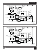
Figure 3. Pin Configuration (top view).
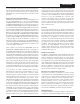
PI-2509-040501
DC
Input
Voltage
+
-
DM
S
C
V
UV
= I
UV
x R
LS
V
OV
=
I
OV
x
R
LS
For R
LS
= 2 MΩ
V
UV
= 100 VDC
V
OV
=
450 VDC
DC
MAX
@100 VDC = 78%
DC
MAX
@375 VDC = 38%
CONTROL
R
LS
2 MΩ
PI-2517-040501
DC
Input
Voltage
+
-
DM
S
C
For R
IL
= 12 kΩ
I
LIMIT
= 69%
CONTROL
R
IL
See fig. 55 for other
resistor values (R
IL
)
For R
IL
= 25 kΩ
I
LIMIT
= 43%
to select different
I
LIMIT
values
X
PI-2629-040501
DC
Input
Voltage
+
-
D
S
C
CONTROL
L
R
IL
R
LS
12 kΩ
2 MΩ
V
UV
= I
UV
x R
LS
V
OV
=
I
OV
x
R
LS
For RLS =
2
MΩ
DC
MAX
@100 VDC = 78%
DC
MAX
@375 VDC = 38%
For R
IL
= 12 kΩ
I
LIMIT
= 69%
See fig. 55 for other
resistor values (R
IL
)
to select different I
LIMIT
values
V
UV
= 100 VDC
V
OV
= 450 VDC
Figure 4. Y/R/F Package Line Sense and Externally Set Current
Limit.
Figure 5. P/G Package Line Sense.
Figure 6. P/G Package Externally Set Current Limit.
FREQUENCY (F) Pin: (Y, R or F package only)
Input pin for selecting switching frequency: 132 kHz if
connected to SOURCE pin and 66 kHz if connected to
CONTROL pin. The switching frequency is internally set for
fixed 132 kHz operation in P and G packages.
SOURCE (S) Pin:
Output MOSFET source connection for high voltage power
return. Primary side control circuit common and reference point.
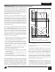
PI-2724-010802
Tab Internally
Connected to
SOURCE Pin
Y Package (TO-220-7C)
C
D
S
S
S
S
1 C
3 X
2 L
5 F
4 S
7 D
M
P Package (DIP-8B)
G Package (SMD-8B)
R Package (TO-263-7C)
F Package (TO-262-7C)
8
5
7
1
12345 7
CLXS F D
4
2
3