
Datasheet


TOP242-250
34
I
4/03
General Information & Table of Contents
Product Selector Guide 1
Data Sheets 2
Application Notes 3
Design Ideas 4
Design Tools 5
Quality and Reliability 6
Package Information 7
DPA-Switch
DC-DC Seminar 8
LinkSwitch
&
TinySwitch-II
AC-DC Seminar 9
TOPSwitch-GX
AC-DC Seminar 10
Sales Representatives and Distributors 11
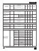
ABSOLUTE MAXIMUM RATINGS
(1)
DRAIN Voltage ............................................ -0.3 to 700 V
DRAIN Peak Current: TOP242 ...............................0.72 A
TOP243 ...............................1.44 A
TOP244 ...............................2.16 A
TOP245 ...............................2.88 A
TOP246 ...............................4.32 A
TOP247 ...............................5.76 A
TOP248 ...............................7.20 A
TOP249 ...............................8.64 A
TOP250 .............................10.08 A
CONTROL Voltage .......................................... -0.3 to 9 V
I
C
= 3 mA;
T
J
= 25 °C
f
OSC
DC
(ONSET)
f
OSC (DMIN)
∆f
f
M
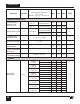
CONTROL FUNCTIONS
Conditions
(Unless Otherwise Specified)
See Figure 53
SOURCE = 0 V; T
J
= -40 to 125 °C
Min Typ Max
Parameter
Symbol
Units
THERMAL IMPEDANCE
kHz
%
kHz
kHz
Hz
Thermal Impedance: Y or F Package:
(θ
JA
)
(1)
....................................... 80 °C/W
(θ
JC
)
(2)
......................................... 2 °C/W
P or G Package:
(θ
JA
) ......................70 °C/W
(3)
; 60 °C/W
(4)
(θ
JC
)
(5)
....................................... 11 °C/W
R Package:
(θ
JA
) ... 80 °C/W
(7)
; 40 °C/W
(4)
; 30 °C/W
(6)
(θ
JC
)
(5)
......................................... 2 °C/W
Notes:
1. Free standing with no heatsink.
2. Measured at the back surface of tab.
3. Soldered to 0.36 sq. inch (232 mm
2
), 2 oz. (610 gm/m
2
) copper clad.
4. Soldered to 1 sq. inch (645 mm
2
), 2 oz. (610 gm/m
2
) copper clad.
5. Measured on the SOURCE pin close to plastic interface.
6. Soldered to 3 sq. inch (1935 mm
2
), 2 oz. (610 gm/m
2
) copper
clad.
7. Soldered to foot print area, 2 oz. (610 gm/m
2
) copper clad.
124 132 140
61.5 66 70.5
10
30
15
± 4
± 2
250
FREQUENCY Pin
Connected to SOURCE
FREQUENCY Pin
Connected to CONTROL
132 kHz Operation
66 kHz Operation
Switching
Frequency
(average)
Duty Cycle at
ONSET of Fre-
quency Reduction
Switching
Frequency near
0% Duty Cycle
Frequency Jitter
Deviation
Frequency Jitter
Modulation Rate
132 kHz Operation
66 kHz Operation
CONTROL Current ...............................................100 mA
LINE SENSE Pin Voltage ................................ -0.3 to 9 V
CURRENT LIMIT Pin Voltage ..................... -0.3 to 4.5 V
MULTI-FUNCTION Pin Voltage .................... -0.3 to 9 V
FREQUENCY Pin Voltage............................... -0.3 to 9 V
Storage Temperature ..................................... -65 to 150 °C
Operating Junction Temperature
(2)
............... -40 to 150 °C
Lead Temperature
(3)
............................................... 260 °C
Notes:
1. All voltages referenced to SOURCE, T
A
= 25 °C.
2. Normally limited by internal circuitry.
3. 1/16" from case for 5 seconds.