
Datasheet


TOP221-227
D
7/01
3
TOPSwitch-II
Family Functional Description
TOPSwitch is a self biased and protected linear control current-
to-duty cycle converter with an open drain output. High
efficiency is achieved through the use of CMOS and integration
of the maximum number of functions possible. CMOS process
significantly reduces bias currents as compared to bipolar or
discrete solutions. Integration eliminates external power
resistors used for current sensing and/or supplying initial start-
up bias current.
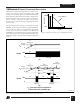
During normal operation, the duty cycle of the internal output
MOSFET decreases linearly with increasing CONTROL pin
current as shown in Figure 4. To implement all the required
control, bias, and protection functions, the DRAIN and
CONTROL pins each perform several functions as described
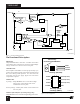
below. Refer to Figure 2 for a block diagram and to Figure 6 for
timing and voltage waveforms of the TOPSwitch integrated
circuit.
PI-2040-050197
D
MAX
D
MIN
Duty Cycle (%)
I
C
(mA)
2.0 6.0
Slope = PWM Gain
I
B
I
CD1
Auto-restart
Figure 4. Relationship of Duty Cycle to CONTROL Pin Current.
DRAIN
0
V
IN
V
C
0
4.7 V
5.7 V
8 Cycles
95%
5%
Off
Switching Switching
Off
I
C
Charging C
T
I
CD1
Discharging C
T
I
CD2
Discharging C
T
I
C
Charging C
T
Off
PI-1956-092496
DRAIN
0
V
IN
V
C
0
4.7 V
5.7 V
Off
Switching
(b)
(a)
C
T
is the total external capacitance
connected to the CONTROL pin
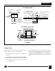
Figure 5. Start-up Waveforms for (a) Normal Operation and (b) Auto-restart.