
Datasheet


TOP221-227
D
7/01
2
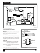
Figure 2. Functional Block Diagram.
Pin Functional Description
DRAIN Pin:
Output MOSFET drain connection. Provides internal bias
current during start-up operation via an internal switched high-
voltage current source. Internal current sense point.
CONTROL Pin:
Error amplifier and feedback current input pin for duty cycle
control. Internal shunt regulator connection to provide internal
bias current during normal operation. It is also used as the
connection point for the supply bypass and auto-restart/
compensation capacitor.
SOURCE Pin:
Y package – Output MOSFET source connection for high
voltage power return. Primary side circuit
common and reference point.
P and G package – Primary side control circuit common and
reference point.
SOURCE (HV RTN) Pin: (P and G package only)
Output MOSFET source connection for high voltage power return.
PI-1935-091696
SHUTDOWN/
AUTO-RESTART
PWM
COMPARATOR
CLOCK
SAW
OSCILLATOR
CONTROLLED
TURN-ON
GATE
DRIVER
INTERNAL
SUPPLY
5.7 V
4.7 V
SOURCE
S
R
Q
Q
D
MAX
-
+
CONTROL
-
+
5.7 V
I
FB
R
E
Z
C
V
C
MINIMUM
ON-TIME
DELAY
+
-
V
I
LIMIT
LEADING
EDGE
BLANKING
POWER-UP
RESET
S
R
Q
Q
÷ 8
0
1
THERMAL
SHUTDOWN
SHUNT REGULATOR/
ERROR AMPLIFIER
+
-
DRAIN
PI-2084-040401
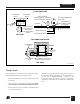
CONTROL
DRAIN
SOURCE
Y Package (TO-220/3)
Tab Internally
Connected to SOURCE Pin
CONTROL
8
5
7
6
DRAIN
SOURCE (HV RTN)
SOURCE
SOURCE
1
4
2
3
SOURCE (HV RTN)
SOURCE (HV RTN)
SOURCE
P Package (DIP-8)
G Package (SMD-8)
Figure 3. Pin Configuration.