
Datasheet


18
F
4/06
TNY274-280
NOTES:
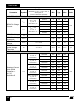
A. I
S1
is an accurate estimate of device controller current consumption at no-load, since operating frequency is so
low under these conditions. Total device consumption at no-load is the sum of I
S1
and I
DSS2
.
B Since the output MOSFET is switching, it is difficult to isolate the switching current from the supply current at the
DRAIN. An alternative is to measure the BP/M pin current at 6.1 V.
C. BP/M pin is not intended for sourcing supply current to external circuitry.
D. To ensure correct current limit it is recommended that nominal 0.1 µF / 1 µF / 10 µF capacitors are used. In
addition, the BP/M capacitor value tolerance should be equal or better than indicated below across the ambient
temperature range of the target application. The minimum and maximum capacitor values are guaranteed by
characterization.
E. For current limit at other di/dt values, refer to Figure 23.
F. TNY274 does not set an increased current limit value, but with a 10 µF BP/M pin capacitor the current limit is the
same as with a 1 µF BP/M pin capacitor (reduced current limit value).
G. This parameter is derived from characterization.
H. This parameter is derived from the change in current limit measured at 1X and 4X of the di/dt shown in the I
LIMIT
specification.
I. I
DSS1
is the worst case OFF state leakage specification at 80% of BV
DSS
and maximum operating junction
temperature. I
DSS2
is a typical specification under worst case application conditions (rectified 265 VAC) for no-load
consumption calculations.
J. Breakdown voltage may be checked against minimum BV
DSS
specification by ramping the DRAIN pin voltage up
to but not exceeding minimum BV
DSS
.
K. Auto-restart on time has the same temperature characteristics as the oscillator (inversely proportional to
frequency).
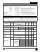
Nominal BP/M
Pin Cap Value
Tolerance Relative to Nominal
Capacitor Value
Min MAX
0.1 µF -60% +100%
1 µF -50% +100%
10 µF -50% NA