
Datasheet


12
F
4/06
TNY274-280
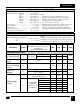
either from no-clean flux or other contaminants, can reduce the
surface resistivity enough to allow parasitic currents >1 µA to
flow into the EN/UV pin. These currents can flow from higher
voltage exposed solder pads close to the EN/UV pin such as the
BP/M pin solder pad preventing the design from starting up.
Designs that make use of the under-voltage lockout feature by
connecting a resistor from the high voltage rail to the EN/UV
pin are not affected.
If the contamination levels in the PC board assembly facility
are unknown, the application is open frame or operates in a high
pollution degree environment and the design does not make use
of the under-voltage lockout feature, then an optional 390 kΩ
resistor should be added from EN/UV pin to SOURCE pin to
ensure that the parasitic leakage current into the EN/UV pin
is well below 1 µA.
Note that typical values for surface insulation resistance (SIR)
where no-clean flux has been applied according to the suppliersʼ
guidelines are >>10 MΩ and do not cause this issue.
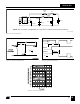
Quick Design Checklist
As with any power supply design, all TinySwitch-III designs
should be verified on the bench to make sure that component
specifications are not exceeded under worst case conditions. The
following minimum set of tests is strongly recommended:
1. Maximum drain voltage – Verify that V
DS
does not exceed
650 V at highest input voltage and peak (overload) output
power. The 50 V margin to the 700 V BV
DSS
specification
gives margin for design variation.
2. Maximum drain current – At maximum ambient temperature,
maximum input voltage and peak output (overload) power,
verify drain current waveforms for any signs of transformer
saturation and excessive leading edge current spikes at
startup. Repeat under steady state conditions and verify that
the leading edge current spike event is below I
LIMIT(Min)
at the
end of the t
LEB(Min)
. Under all conditions, the maximum drain
current should be below the specified absolute maximum
ratings.
3. Thermal Check – At specified maximum output power,
minimum input voltage and maximum ambient temperature,
verify that the temperature specifications are not exceeded
for TinySwitch-III, transformer, output diode, and output
capacitors. Enough thermal margin should be allowed for
part-to-part variation of the R
DS(ON)
of TinySwitch-III as
specified in the data sheet. Under low line, maximum power,
a maximum TinySwitch-III SOURCE pin temperature of
110 °C is recommended to allow for these variations.