
Datasheet


11
TNY274-280
F
4/06
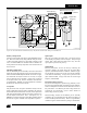
Primary Clamp Circuit
A clamp is used to limit peak voltage on the DRAIN pin at turn
off. This can be achieved by using an RCD clamp or a Zener
(~200 V) and diode clamp across the primary winding. In all
cases, to minimize EMI, care should be taken to minimize the
circuit path from the clamp components to the transformer and
TinySwitch-III.
Thermal Considerations
The four SOURCE pins are internally connected to the IC lead
frame and provide the main path to remove heat from the device.
Therefore all the SOURCE pins should be connected to a copper
area underneath the TinySwitch-III to act not only as a single
point ground, but also as a heatsink. As this area is connected
to the quiet source node, this area should be maximized for
good heatsinking. Similarly for axial output diodes, maximize
the PCB area connected to the cathode.
Y-Capacitor
The placement of the Y-capacitor should be directly from the
primary input filter capacitor positive terminal to the common/
return terminal of the transformer secondary. Such a placement
will route high magnitude common mode surge currents away
from the TinySwitch-III device. Note – if an input π (C, L, C)
EMI filter is used then the inductor in the filter should be placed
between the negative terminals of the input filter capacitors.
Optocoupler
Place the optocoupler physically close to the TinySwitch-III
to minimizing the primary-side trace lengths. Keep the high
current, high voltage drain and clamp traces away from the
optocoupler to prevent noise pick up.
Output Diode
For best performance, the area of the loop connecting the
secondary winding, the output diode and the output filter
capacitor, should be minimized. In addition, sufficient copper
area should be provided at the anode and cathode terminals
of the diode for heatsinking. A larger area is preferred at the
quiet cathode terminal. A large anode area can increase high
frequency radiated EMI.
PC Board Leakage Currents
TinySwitch-III is designed to optimize energy efficiency across
the power range and particularly in standby/no-load conditions.
Current consumption has therefore been minimized to achieve
this performance. The EN/UV pin under-voltage feature for
example has a low threshold (~1 µA) to detect whether an
under-voltage resistor is present.
Parasitic leakage currents into the EN/UV pin are normally
well below this 1 µA threshold when PC board assembly is in
a well controlled production facility. However, high humidity
conditions together with board and/or package contamination,
Figure 15. Recommended Circuit Board Layout for TinySwitch-III with Under-Voltage Lock Out Resistor.
TOP VIEW
PI-4368-042506
Opto-
coupler
+
-
HV
+-
DC
OUT
Input Filter Capacitor
Output
Rectifier
Safety Spacing
T
r
a
n
s
f
o
r
m
e
r
PRI
SEC
BIAS
D
Output Filter
Capacitor
Maximize hatched copper
areas ( ) for optimum
heatsinking
BP/M
EN/UV
Y1-
Capacitor
S
S
S
S
PRI
C
BP
BIAS
TinySwitch-III