
Datasheet


D
4/03
TNY253/254/255
12
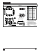
NOTES:
A. For a threshold with a negative value, negative hysteresis is a decrease in magnitude of the corresponding threshold.
B. Total current consumption is the sum of I
S1
and I
DSS
when ENABLE pin is shorted to ground (MOSFET not switching)
and the sum of I
S2
and I
DSS
when ENABLE pin is open (MOSFET switching).
C. Since the output MOSFET is switching, it is difficult to isolate the switching current from the supply current at the
DRAIN. An alternative is to measure the BYPASS pin current at 6.2 V.
D. Bypass pin is not intended for sourcing supply current to external circuitry.
E. See typical performance characteristics section for BYPASS pin start-up charging waveform.
F. For current limit at other di/dt values, refer to current limit vs. di/dt curve under typical performance
characteristics.
G. This parameter is derived from the change in current limit measured at 5X and 10X of the di/dt shown in the I
LIMIT
specification.
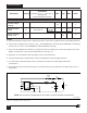
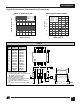
Figure 14. TinySwitch General Test Circuit.
PI-2211-061898
0.1 µF
10 V
50 V
470 Ω
5 W
S2
S1
470 Ω
NOTE: This test circuit is not applicable for current limit or output characteristic measurements.
DEN
BPS
S
S
S
S
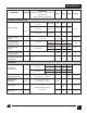
Conditions
Parameter Symbol SOURCE = 0 V; T
J
= -40 to 125 °C
See Figure 14
(Unless Otherwise Specified)
50
0.5
t
EN
t
DST
V
µs
µs
DRAIN Supply
Voltage
Output Enable
Delay
Output Disable
Setup Time
Min
Typ
Max
Units
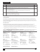
OUTPUT (cont.)
See Figure 16
TNY253
TNY254
TNY255
10
14